Intel 8254 is a programmable interval timer designed by intel is a programmable external timer device built with an aim to resolve the time control issues that occur in between various processes occurring within the microprocessor. In order to communicate with the processor, it has a total of 8 data lines.
There are overall 24 pin signals in which it operates and the power supply provided to it is +5V.
Content: Programmable Interval Timer
Introduction
We know that multiple operations take place within the processor and thus it is necessary that timing between the various operations must be managed properly. When time-based actions occur within the system then for proper controlling of the timing of the operations, in general, there are two methods. The two methods are as follows:
- Delay subroutine is executed by the processor: In this case, a count value will be stored in one of the processor’s registers by the delay subroutine and the count value will start to decrement one after the other. However, here zero flags must be properly monitored after each decrement so as to check whether the count has reached 0 or not.
Once the zero flag shows high then this corresponds to 0 of the count value and the delay subroutine gets terminated. After this, the processor can execute the specific time-based operation. The time in which the delay subroutine is executed depends on the time decided by the processor in terms of the clock period. - The external timer is used to maintain timing: In this case, the timer interrupts the processor at periodic intervals. This method offers efficient processor utilization as unnecessarily processor is not busy in decrementing the value count of the register. Here in this method, the interrupts get generated automatically so the processor can execute other tasks in the intermediary durations.
Intel 8254 is an external timer that maintains the timing of the processor operations. It is known to be an advancement of 8253. The Intel 8254 has three counters that operate independently. Each counter is of 16-bit value and can handle clock input up to 10 MHz.
It is known to be a general-purpose, multi-timing element that forms an array of I/O ports in system software. Through this accurate timing, delays can be obtained under software controlling as once delay tenure has been completed then 8254 interrupts the CPU.
Features offered by Programmable Interrupt Timer
- When an operating system is working on a time-sharing basis then the timer enables smooth operation while switching programs using an interrupt.
- The timer behaves as a counter that serves the purpose of an external event counter that counts the repetitive external operations and provides the overall count to the processor.
- It is used to measure the time difference between two external events.
- It acts as a baud rate generator (i.e., free running counters that generate an internal clock).
- The timer enables the processor to initiate a new operation after a sequence of external events has occurred.
- Through timer, timing signals can be sent to the IO devices at periodic intervals.
Block Diagram of Intel 8254
The figure down below shows the functional block diagram of 8254 Timer:
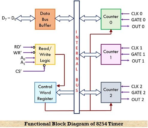
We have already discussed in the beginning that it consists of a total of 3 counters of 16-bit each and adequate programming is performed so that each one operates properly in one of the six possible modes. It has 2 inputs namely clock and gate while 1 output i.e., counter. The counter operates in a way that initially a count value is stored in the count register and at this time gate signal will be high and input is provided through clock input. After each cycle of the clock input, the counter decrements the value by 1, and output is obtained according to the mode of operation.
Here overall 8 data lines are there through which 8254 communicates with the processor. Through the data bus buffer, registers store the control words and count values. The read and write operations are performed through control signals RD’ and WR’. Out of the four internal devices i.e., the three counters and a control register, anyone is selected using address lines A0 and A1.
It is to be noted here that there is another timer called Intel 8253 which offers a clock frequency of 2.6 MHz. Thus is regarded as a low clock version of 8254. Both of these function in a similar manner however, the only difference exists in their operating clock frequency.
Programming of 8254
At the time of programming the timer it is necessary that each individual counter of 8254 is to be programmed separately using control word and count value.
The figure below shows the format of the control word:
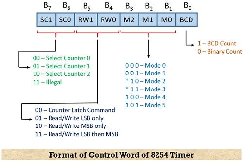
Here in the control word format, B0 selects the BCD or binary count while B1, B2, and B3 are used to select one of the modes of operation for the counter which bits B6 and B7 specify. For the operation to take place, the control word is needed to be sent for each separate counter at the same control address register. The identification of the control word of the particular counter is done using bits B6 and B7 of the control word format.
The read/ write operations are performed using bits B4 and B5. Through these bits, the 16-bit count value is read and written in an orderly sequence. Also, each time the read operation will take place the count value is to be read by stopping the counter. Here basically the count value is latched to an internal latch present at the output of each counter before the read operation.
Unlike 8253, there is a separate read-back control word format in 8254 through which the count value is latched. The figure given below shows the format of the read-back control word of 8254:
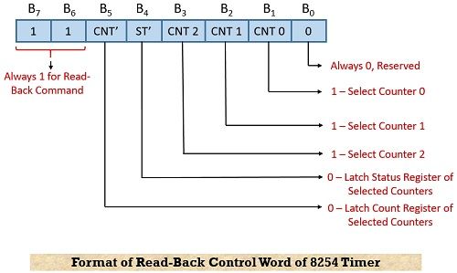
In order to latch the count value before the read operation takes place the control word is sent to the same control register address. The control word is identified using the bit values of B6 and B7 by the control register. By sending one control word, one or all the counters can be latched by the read-back control word. The status register is also latched to the output latch of the counters through the control word, this allows reading the status register by the respective address of the counter.
It is to be noted here that at any specific instant either one can latch the count value by programming the bit B5 as zero or latch the status register by programming the bit B4 as zero.
Below is shown the format of the status register of each counter:
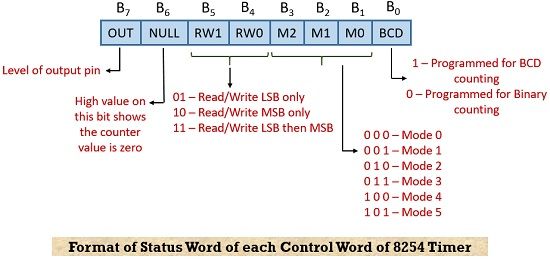
The programmed status of the counter is judged by the status word of the counter and through this one can also check whether the count value has become zero or not.
Pin Description of 8254
The figure here shows the representation of 24 pins IC packed in DIP:
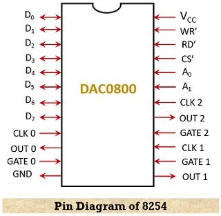
Here D0 to D7 represents the bidirectional 3 states data bus lines used for I/O operations. Vcc represents the power supply connection of +5V while GND corresponds to ground. There are CLK 0 and OUT 0 which is used for clock input of counter 0 and output of counter 0. Similarly, CLK 1 and CLK 2 are the clock inputs of counter and 2 whereas OUT 1 and OUT 2 are outputs. Other than these GATE 0 and GATE 1 pins correspond to the gate input of counter 0 and counter 1 whereas OUT 0 and OUT 1 are the outputs of counter 0 and 1.
A0 and A1 are the address lines by which selection of one of the three counters or the control word register is done for the read/write operation to take place.
| A1 | A0 | Device Selected |
|---|---|---|
| 0 | 0 | Counter 0 |
| 0 | 1 | Counter 1 |
| 1 | 0 | Counter 2 |
| 1 | 1 | Control Register |
WR’ represents the write control pin which is kept at a low signal during the CPU write operations. RD’ is for read control and is low at the time when the CPU performs the read operation. Another crucial pin is the chip select denoted by CS’ and whenever it is low then the timer responds to the read and write signals otherwise such signals are ignored.