Definition: A Phototransistor is a device that has the ability to detect the level of the incident radiation and accordingly change the flow of electric current between emitter and collector terminal. It is a 3-layer semiconductor device that consists of a light sensitive base region. It is basically a transistor whose action depends on the application of light. Hence named phototransistor.
The phototransistor is basically an enhancement of Photodiode. Both photodiode and phototransistor are light sensing device but the sensitivity of phototransistor is somewhat more as compared to the photodiode. As phototransistor has the ability to give larger gain than that of the photodiode. It is similar to a normal BJT but the only variation is that in phototransistor, virtually the base region exists but it is kept unconnected with the external supply.
This means that as in normal BJT, base current is used to drive the circuit, however, in phototransistor light energy falling on the base region acts as the overall input of the device.
A phototransistor is said to exhibit the combined operation of the photodiode as well as a normal transistor. It operates on the principle of Photoelectric effect. As it changes light signal incidenting on its surface into its electrical equivalent form. And the transistor action permits it to perform amplification of the current flowing through it.
Content: Phototransistor
Construction of Phototransistor
As we have already discussed that a phototransistor is nothing but a normal transistor whose action depends on the incident radiation falling at its base. At the time of constructing the phototransistor, the base and collector region is provided with a larger area in comparison to a normal BJT.
The figure below represents the constructional structure of an NPN Phototransistor:
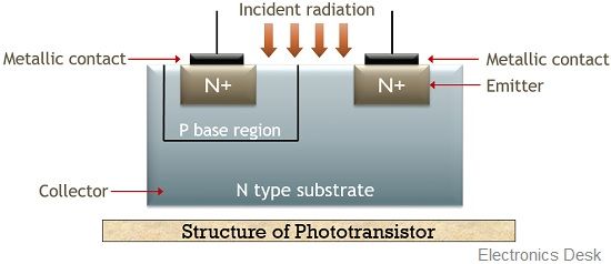
Here, as we can see that the light is majorly allowed to incident at the base collector junction. Initially, phototransistors were fabricated from silicon or germanium as their basic material that resultantly provides homojunction structure. However, in recent times, these are constructed using materials likes gallium or arsenide. Thereby, providing a heterojunction structure. This is so because these structures exhibit large conversion efficiency. This implies they are more capable of changing light energy into electrical energy as compared to homojunction transistors.
Phototransistors are mainly enclosed in a metallic case that consists of the lens at the top in order to gather the incident radiation.
Symbol of Phototransistor
The figure below represents the symbolic representation of a Phototransistor: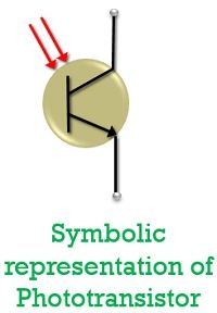
Here, the symbolic representation is almost similar to a normal BJT but the only variation is the presence of two inward arrows at the base region that shows the incident of light radiation.
Working of Phototransistor
The operation of a phototransistor depends on the intensity of radiation falling at its base region. Its working is almost similar to a normal transistor, however; the variation lies in the input current that drives the circuit. And in the case of a phototransistor, the incident light generates driving current.
The figure below represents the biasing arrangement of a phototransistor:
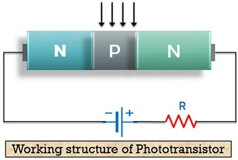
In the circuit arrangement, we can clearly see that the base region is kept unconnected with the external supply voltage and is used as the region for radiation incidence. Only the collector region is connected to the positive side of the supply provided along with emitter which is connected to the negative side. However, the output is taken at the emitter terminal of the transistor.
When no any light is allowed to incident at the base region of the transistor, the due to temperature variation, movement of minority carriers across the junction generates a very small current through the transistor which is reverse saturation current basically termed as dark current. Here, the base current IB is majorly 0. Here, in this case, the output current will be less as compared to supply provided. But, when a certain amount of light energy is allowed to fall at the base of the transistor, then electron and hole pair gets generated. The applied electric field causes the electrons to move into the emitter region, thereby generating large electric current.
The figure below represents the circuit of a phototransistor:
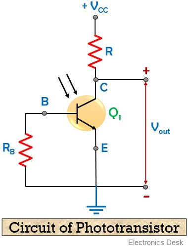
As the intensity of the light falling at the base region is increased, the current through the device also increases. Here, the generated photocurrent majorly depends on the illumination provided to the base.
Characteristics Curve of Phototransistor
The figure below represents the characteristics curve of phototransistor:
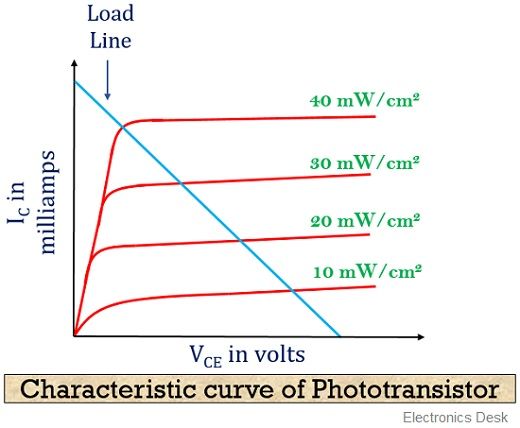
Here x-axis represents the voltage applied at the collector-emitter terminal of the transistor and the y-axis represents the collector current that flows through the device in mill amperes. As all the curves in the above figure are clearly indicating that current increases with the intensity of the radiation that falls at the base region.
Also, the figure below represents the variation in the base current with the variation in the light intensity.
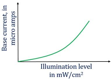
Here, the x-axis represents the illumination level whereas y-axis represents the equivalent base current generated.
Advantages of Phototransistor
- These are a highly sensitive optoelectronic device.
- It is less complex and inexpensive.
- Phototransistors provides a large output current with high gain.
Disadvantages of Phototransistor
- It provides a low-frequency response.
- In the case when a small amount of illumination is provided, the circuit is not able to detect it effectively.
- Electric surges are more severe in phototransistors rather than a photodiode.
- Phototransistors gets affected by the variation in electromagnetic energy.
Applications of Phototransistor
The applications of phototransistors are as follows:
- In light controlling and detection: As phototransistors are a very sensitive light detector. Thus these are widely used in light detection and controlling applications.
- In an indication of level and relays: The device finds its uses in indicating the level of some systems because of their light sensing ability.
- In counting systems: Phototransistors can be effectively utilized in counting systems. As it has tremendous ability to combinely operate as photodiode and transistors. Thus, failure of supply will not cause much adverse effects on the system.
- In punch card readers: Phototransistors widely finds its applications in punch card reading.
Key terms related to Phototransistor
- Photodiode: Photodiode is a semiconductor device having two terminals that generates electric current when the pn junction is illuminated with light energy. It operates on the principle of the photoelectric effect.
- Dark current: It the reverse current that flows through the device when no any light energy is supplied to the device. This current mainly flows due to the movement of minority charge carriers.
- BJT: BJT is the abbreviation used for bipolar junction transistor. It is a 3 terminal device, emitter, base and collector that is used for switching and amplification.
Though phototransistors are highly sensitive devices, the device is somewhat slow. This clearly means that with the increased sensitivity a major drawback is concerned regarding its on and off time.
Thank u. Very helpful to me.