Both NPN and PNP transistors are the two major classifications of Bipolar Junction Transistor (BJT). However, there exist several differences between the two. One of the major differences between NPN and PNP transistor is that in NPN transistors, electrons are the majority carriers, hence electrons are responsible for current flow. While, in PNP transistors, holes are the majority carriers, hence current flows due to the movement of holes.
NPN transistor is the acronym used for Negative-Positive-Negative transistors. As against, PNP transistor is an acronym used for Positive-Negative-Positive transistor.
Let’s see the contents to be discussed under this article and then we will move further in order to understand other major differences between the two.
Content: NPN Vs PNP Transistor
Comparison Chart
| Parameter | NPN Transistor | PNP Transistor |
|---|---|---|
| Full form | Negative-Positive-Negative | Positive-Negative-Positive |
| Symbolic representation | 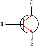 | 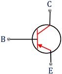 |
| Majority carriers | Electrons | Holes |
| Direction of flow of electric current | From collector to emitter | From emitter to collector |
| Minority carriers | Holes | Electrons |
| Mobility of majority carriers | High | Low |
| Conductivity Level | High | Low |
| Sandwiched region | P region | N region |
| Frequency response | Fast | Comparatively slow than NPN transistor. |
| Supply provided to emitter | Negative | Positive |
| Supply provided to collector | Positive | Negative |
Definition of NPN Transistor
NPN is the abbreviation used for Negative-Positive-Negative transistor. It is a 3-layer device namely emitter, base and collector.
The figure below represents the NPN transistor with biasing arrangement:
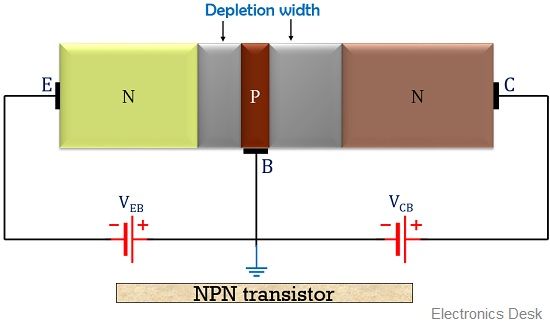
Here, the leftmost n region shows the emitter region, the middle p region shows the base region and the rightmost n region shows the collector region. In an NPN transistor, p-region is sandwiched between two n regions. In NPN transistor, electrons are the majority carriers and holes are the minority carriers.
The applied forward biased voltage at the emitter-base junction allows the electrons to move into the base region after overcoming the barrier potential at the EB junction.
As the negative terminal of the battery connected to the n region applies a repulsive force to the electrons present in the n region. And on reaching the base region only a few electrons get combined with the holes present in that region. Rest move towards the collector region, and as we can see clearly in the above figure, that collector region is connected with the positive terminal of the battery. Hence, this positive potential attracts electrons from the base region. Thus, in this way current flows from collector to emitter i.e., in the reverse direction of the movement of electrons.
Among the 3 regions, the collector region has a larger area but it is moderately doped. While the emitter region is the second-largest but is highly doped. On the other side, the base region has the smallest area and is lightly doped.
Definition of PNP Transistor
PNP is the abbreviation used for the positive-negative-positive transistor. It also consists of an emitter, base and collector region.
The figure below represents the PNP transistor with biasing arrangement:
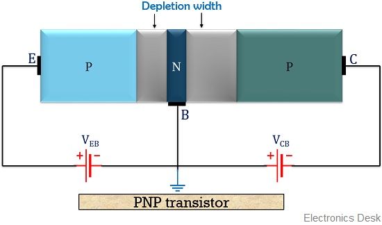
In PNP transistor, n region is sandwiched between two p regions. Here, holes acts as majority carriers and electrons are the minority carriers.
As the forward voltage is provided at the emitter-base junction of the transistor. Thus, the positive potential of the battery applies repulsion to the holes present in the p region. These holes on experiencing repulsive force move towards the lightly doped base region. While the base is lightly doped hence very small amount of moving holes gets combined with the electrons of the base region. Rest drift towards the collector. Also, the collector region is connected to the negative terminal of the battery, hence the negative terminal attracts holes drifting towards the collector region. Thus, in this way, current flows from emitter to collector i.e., in the direction of the movement of holes.
Here also, among the 3 regions, the emitter is highly doped but has moderate in size. While the collector is doped at a moderate level but it has the greatest size among all the regions.
Key Differences Between NPN and PNP Transistor
- The factor that generates a key difference between NPN and PNP transistor is that in NPN transistor due to sandwiching of p region between two n regions electrons are the majority carriers. While in PNP transistor due to sandwiching of the n region between two p regions holes acts as majority carriers.
- In NPN transistors, the current flows from collector to emitter terminal i.e., opposite to the direction of movement of electrons. As against, in PNP transistors, the current flows from emitter to collector terminal.
- In the symbolic representation of NPN transistor, an outward arrow from the base towards emitter represents the direction of flow of current. However, the symbolic representation of PNP transistor an inward arrow from emitter towards base shows the direction of flow of current.
- An npn transistor exhibits faster frequency response as compared to a pnp transistor.
- In NPN transistor holes are the minority carriers while in PNP transistor electrons are the minority carriers.
- The conductivity level of NPN transistor is somewhat high as compared to PNP transistor. This is so because electrons are more mobile than holes. So, their movement in NPN transistor generates high conduction.
- Also, the two types of BJT shows variation with respect to their biasing arrangement. As the voltage provided to the emitter of NPN transistor is negative and to that of PNP transistor is positive. Also, the voltage provided to the collector of NPN transistor is positive and to that of PNP is negative.
Similarity
In both NPN and PNP transistors emitter-base junction is always provided forward potential and the collector-base junction is always provided reverse voltage biased in order to have proper conduction to take place.
Conclusion
So, from the above discussion, we can conclude that both NPN and PNP are the two configurations of BJT and responsible for current amplification and switching. These are current controlled devices. But, the presence of different majority carriers shows variation in their working principle.