Definition: NPN transistor is a type of bipolar transistor that has 3 layers and is used for signal amplification. It is a current controlled device. NPN is an abbreviation used for a negative positive negative transistor. This means a p-type semiconductor is fused between 2 n-type semiconductor material.
It has 3 regions namely emitter, base and collector. The flow of electrons is responsible for the conduction in NPN transistor.
Content: NPN Transistor
Symbol of NPN transistor
The figure below shows the symbolic representation of the NPN transistor:
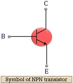
In the symbolic representation, the outward arrow at the emitter terminal clearly shows the direction of flow of current through the device. In NPN transistor the majority carriers are electrons.
Construction of NPN transistor
As we are already familiar with the fact that NPN transistor is formed when a p-type semiconductor material (either Silicon or Germanium) is fused between two n-type semiconductor material.
The figure below represents the constructional structure of NPN transistor:
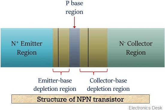
It has basically 3 regions i.e., emitter, base and collector.
The junction region present between emitter and base region is termed as the emitter-base junction. Similarly, the junction region between the base and collector region is termed as the collector-base junction. Due to the presence of 2 junctions in between 3 regions, it acts like 2 PN junction diodes.
The doping levels of all the 3 regions are different. The emitter region is highly doped; the base region is lightly doped. And the doping level of collector region falls in between the emitter and base region or we can say its doping level is moderate.
It is noteworthy here that we cannot interchange the emitter and collector region. The reason for this is that the thickness of the collector region is somewhat greater than the emitter region. So, that it can dissipate more power.
Working of NPN transistor
Let us now understand how NPN transistor operates.
When the transistor is not provided with any applied bias or when no battery is connected between its terminals. Then it is said to be the unbiased state of the transistor. We have already discussed how a PN junction diode operates under no biased condition. And we already know that a transistor is formed by two PN junction.
So, due to variation in temperature under no biased condition electrons in the emitter region starts moving towards the base region. But, after a certain point of time a depletion region is created at the emitter-base junction of the transistor. After reaching the base region, only around 5% of electrons combine with the holes in this region, rest drift across the collector region. Similarly, here also after some time a depletion region is created at the base-collector junction of the transistor.
It is to be noted here that the doping concentration of the material is responsible for the thickness or thinness of the depletion region. More clearly, we can say that the width of the depletion region will be more in the case of a lightly doped region in comparison to the highly doped region. This is the reason why we achieve broader depletion width at the collector-base junction than the emitter-base junction. These two depletion regions act as the potential barrier for any further flow of majority carriers.
Moving further, let us now understand the case when a voltage is applied to the terminals of the transistor. Generally, the emitter-base junction is provided forward dc voltage and the collector-base junction is supplied with a reverse dc voltage.
The figure shows the biased condition of NPN transistor:
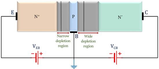
Due to the forward applied voltage at the emitter-base junction, the width of the depletion region gets narrowed. Similarly, the reverse applied voltage broadens the width of the collector-base junction. This is the reason why we have shown a thin depletion region at the emitter-base junction as compared to the collector-base junction in the above figure.
Due to the forward applied voltage VBE, electrons start injecting into the emitter region. The electrons in this region have sufficient energy by which it overcomes the barrier potential of the emitter-base junction to arrive the base region.
The figure below represents that charge carrier movement in NPN transistor:
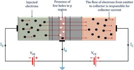
As the base region is very thin and lightly doped. So, after reaching there very few electrons get combined with the holes. Due to the very thin base region and the reverse voltage at the collector-base junction, electrons start to drift at the collector region because of the strong electrostatic field. So, now these electrons get collected at the collector terminal of the transistor.
As recombined holes and electrons get separated from each other, the electrons start moving towards collector. Due to this movement, a very small base current also flows through the device. This is the reason why emitter current is the summation of base current and collector current.
IE = IB + IC
Applications of NPN transistor
- As NPN transistors are used for signal amplification. Thus used in amplifying circuits.
- It also finds its applications in logarithmic converters.
- One of the major advantages of NPN transistor is its switching characteristic. Thus widely used in switching applications.
- These are also used in high-frequency applications.
Key terms related to NPN transistor
- Emitter region: It is left the most section of the structure which has a size greater than base region but less than collector region. It is highly doped. It is used to transfer majority carriers i.e., electrons into the base region. It is a forward biased region that means it is always provided forward biased with respect to the base region.
- Base region: The middle section of the structure is the base region. Its region is small as compared to emitter and collector region of the transistor. It is lightly doped in order to have minimum recombination so as to have large current at the collector.
- Collector region: It is the rightmost section of the structure and its functioning lies in its name itself i.e., it collects the carriers transferred by the base region. Reverse biasing is provided to this region w.r.t base region.
The operation of another type of bipolar transistor i.e., PNP is almost similar to NPN transistor. However, the only variation lies in the majority carriers responsible for current flow and the biasing arrangement provided to it.