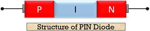
Definition: A PIN diode is an advancement of normal PN junction diode. It is a 3-layer device in which an intrinsic layer i.e., undoped semiconductor is sandwiched between P and N regions. Thus, making it a PIN diode.
The presence of intrinsic region exhibits high resistance property. Due to this, the magnitude of the electric field also becomes large. This resultantly increases the electron and hole pair generation in the region. Hence, it allows the operation of the weak input signal.
It is a type of photodetector that has the ability to change light energy into its electrical form due to the presence of intrinsic region. Along with providing high resistance a PIN diode also possesses a lower value of capacitance. This is so because we know,
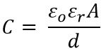
As with the insertion of intrinsic region, the distance between p and n region increases. From the above expression, it is clear that capacitance and distance are inversely proportional. Thus, with the increase in the distance the capacitance decreases.
Content: PIN Diode
Symbol of PIN diode
The figure below represents the symbol of PIN diode:
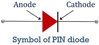
Here, p region denotes the anode terminal and n region denotes the cathode terminal.
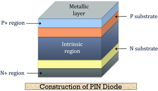
Construction of PIN diode
A PIN diode is a 3-layer device composed of p region, n region and intrinsic region. P region is formed by doping trivalent impurity to the semiconductor. And the n region is formed when the pentavalent impurity is doped to the semiconductor material. The region of an intrinsic semiconductor is nothing but the undoped semiconductor material.
The figure below represents the constructional overview of PIN diode:
A PIN diode is formed by two methods, i.e., either by planar structure or mesa structure.
In case of the mesa structure, the layers of semiconductor which are previously doped are developed (grown) on the intrinsic region. Thereby generating a PIN diode.
In the case of planar structure, a narrow (thin) epitaxial layer is imposed on the intrinsic region in order to form a P+ region. Similarly, N+ region is also created on another side of the substrate. The intrinsic region offers very high resistivity of the order of 0.1 Ω-m.
Working of PIN diode
A PIN diode is almost similar to a normal PN junction diode however the only variation is the presence of intrinsic region. This region is nothing but serves as the depletion region between P and N regions.
When no any external potential is provided to the diode. The carriers diffuse across the junction because of the concentration gradient. Thus, forming a depletion region at NI junction. However, the thickness is greater on the i region as compared to n region. This is so because the doping level of N region is very much higher than I region. As we already assume that the intrinsic region is undoped semiconductor material.
- Forward biased condition:
In case a forward voltage is provided to the diode, the charge carriers from p and n region are injected into the intrinsic region. This is so because applied forward potential reduces the depletion width. Due to this, the resistance offered by the device in no biased condition starts decreasing because of forward biasing. So, as the forward voltage is increased, the greater number of charge carriers gets injected into the intrinsic region.
Thereby, producing a large current through the device and resultantly decreasing the resistance. Hence, it is said that in a forward biased condition PIN diode behaves as a variable resistance device.
- Reverse biased condition:
Now, as the reverse bias voltage is applied to the device. The depletion width starts increasing. As the reverse voltage is increased, the width of the depletion region increases as far as whole mobile carriers swept away from the intrinsic region. This particular voltage is known as swept out voltage. Usually, its value is -2V.
The device functions as a capacitor in a reverse biased condition. Here P and N region serve as the two parallel plates of the capacitor. In case of high reverse bias, a thin depletion region is noticed in the p region.
Characteristics of PIN diode
- Low Capacitance: As we already discussed that a PIN diode offers a lower value of capacitance due to the larger distance between p and n region. When only a small reverse potential is applied, the depletion region gets totally depleted. As the depletion region gets depleted, the capacitance will now do not show variation with the applied potential. Due to the presence of a small amount of charge in the intrinsic region.
- High breakdown voltage: Due to the presence of intrinsic region, PIN diode exhibits a higher value of breakdown voltage. This is so because a higher voltage is required in order to destroy the thick depletion region.
- Sensitive to photodetection: The depletion region is responsible for generating energy when radiation falls on its surface. The existence of an intrinsic region enhances the area for radiation absorption. Hence, these are widely used as photodetectors.
- Storage of carriers: This is the important characteristic of PIN diode. The intrinsic region enhances the area for storage of carriers. The stored charge in the depletion region is responsible for the amount of current flowing through the circuit. When forward biasing is provided to the device, then, in this case, the device exhibits variable resistance characteristics. As the resistance varies with the supplied input voltage. Hence, it does not produce distortion or rectification.
Applications of PIN diode
- As a Photodetector: A PIN diode can change the absorbed light into electrical energy. The placement of intrinsic region between the p and n region increases the region for radiation absorption.
With the increased radiation absorption region, the efficiency of the device to produce electrical energy also increases. Thus, it can be used as a photodiode. - As a radio frequency switch: The intrinsic region isolates the p and n region of the diode due to which capacitance decreases. The capacitance of the device should almost negligible in order to operate it as a switch.
- As a voltage rectifier: PIN diode is able to bear high reverse voltage due to the intrinsic layer. This leads to an increase in the breakdown voltage of the diode. Hence, due to this, the device allows the rectification of high input voltage.
Key terms related to PIN diode
- Swept-out voltage: It is that reverse applied voltage at which the charge carriers get completely swept away from the depletion region. Its value is somewhat -2V.
- Response time: It is the time taken by the device to show change from one state to another. Or we can say, the time taken by the device to change from conducting to non-conducting state or vice-versa.
PIN diode possesses a faster response time. Due to this, these are widely used in microwave applications.