Definition: A Schottky diode is a 2 terminal metal-semiconductor device that is formed by diffusing an n-type semiconductor over a metal. Both metal and n-type semiconductor have electrons as their majority carriers, as almost negligible holes are present in a metal.
As in Schottky diode, only majority charge carrier i.e., electrons are responsible for conduction. Hence it is a unipolar device.
Its other names are Schottky barrier diode or hot carrier diode. The reason why these diodes are called so, is that the majority carriers (electrons) drift from n region to the metallic region with very high energy.
Thus termed as hot carriers and as conduction is due to these hot carriers so the device is known as a hot-carrier diode.
Symbol of Schottky diode
The figure below shows the symbolic representation of the Schottky diode:
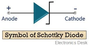
It is clear from the above figure that metal forms the connection as anode and semiconductor region forms the connection as a cathode.
Construction of Schottky Diode
The constructional structure of a Schottky diode shows variation from that of the normal pn junction diode. As we already know that a pn junction diode is formed by merging a p-type semiconductor material with an n-type semiconductor material thereby forming a pn junction diode.
However, for constructing a Schottky diode, an n-type semiconductor material is merged with a metal, so as to have a metal-semiconductor junction.
The figure below represents the constructional structure of a Schottky diode:
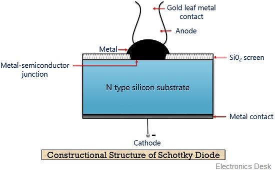
As we can see in the figure shown above that metal is combined with an n-type semiconductor material to form a hot carrier diode. The metal used for fabrication of Schottky diode can be gold, tungsten, platinum silver etc.
On the other side of the metal-semiconductor junction, an n-type semiconductor material is present. Usually, silicon is used as the n-type semiconductor material however, germanium is also used.
The metallic region in the structure acts as an anode while the n-type semiconductor region forms the cathode.
Let us have a look at the structural representation of a Schottky diode:
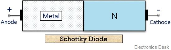
The absence of p-type material with an n-type semiconductor material eliminates the possibility of the presence of a depletion region. Hence preventing the stored charges at the junction.
In case of a Schottky diode, the junction is comparatively more uniform and the device possesses high ruggedness than a point contact diode.
Working of Schottky diode
From the above discussion, it is clear that the operation of a Schottky diode is different from that of a normal diode. So, now let see how conduction takes place in a Schottky diode.
When a metallic region and n-type material forms a connection then the majority charge carriers i.e., electrons move rapidly from the n region to the metallic region. Thereby generating a heavy flow of majority carriers.
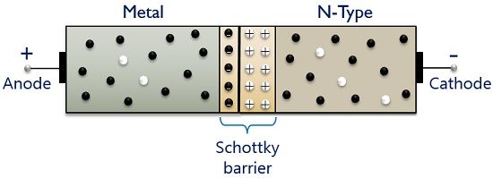
The kinetic energy of these injected carriers is high as compared to the electrons in the metallic region. Thus these are commonly known as hot carriers.
Due to the movement of majority charge carriers from n-type material to metal, a region is generated in the n side near the junction which is depleted (free) of charge carriers. This region is nothing but acts as a surface barrier for further conduction.
The figure above shows the generation of surface barrier in a Schottky diode.
So, in this case, a forward voltage is applied to the device by connecting the positive terminal of the battery with the metal and negative terminal of the battery with the n-type material.
The forward biased condition of a Schottky diode is shown below:
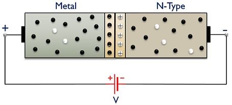
Due to the repulsion from the negative terminal of the battery, the electrons present in the n side move towards the metal side by overcoming the surface barrier. This causes a major flow of electrons across the metal side.
However, the barrier potential in case of a Schottky diode is very less than that of a pn junction diode in forward as well as reverse biased condition.
Therefore, considerably high conduction is noticed in case of a Schottky diode at same applied voltage than a pn junction diode. But this is undesirable in reverse biased condition of Schottky diode as the breakdown is achieved earlier than the pn junction device.
In the reverse biased condition, the negative side of the battery is joined with the metal and the positive side forms a connection with the n-type material.
This is represented in the figure here:
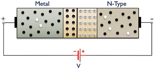
With the applied reverse voltage, the surface barrier increases, due to this the conduction through the device stops.
However, as a greater number of electrons are present in the metal region than the n-type material, then due to an applied reverse voltage, a very small amount of current flows through the device. This is known as leakage current.
On increasing the reverse voltage, the current through it also increases. But after a certain voltage, the increase in applied potential will destroy the surface barrier thereby damaging the diode.
It is noteworthy in the case of Schottky diodes, that the almost negligible presence of holes in the metal decreases the reverse recovery time of the diode. Now, a question comes why this is so?
The answer to the above question is that as we have already discussed that due to the unipolar nature of the device a comparatively smaller barrier potential exists between the two regions. Thus, it can switch off faster than pn junction device. Resultantly reducing the reverse recovery time.
V-I characteristic of Schottky diode
The figure below represents the characteristic curve of a Schottky diode:
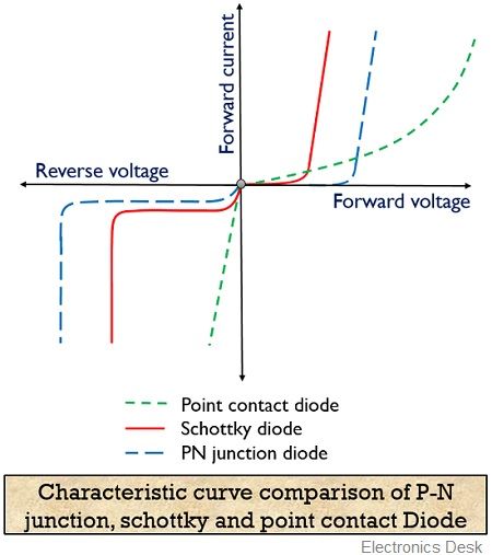
Here, the x-axis shows the applied voltage and the y-axis represents the current flowing through the device. It exhibits barrier potential nearly 0.2 to 0.25 V while it is 0.7 V in case of silicon pn junction diode.
Also, the reverse breakdown voltage in case of Schottky diode is very less than that of a pn junction diode.
Advantages of Schottky Diode
- It possesses low forward turn-on voltage.
- The junction capacitance offered by Schottky diode is low.
- It possesses fast reverse recovery time trr.
- Schottky diodes are highly efficient and are used in high-frequency applications.
Disadvantages of Schottky Diode
- The reverse breakdown voltage is less in case of Schottky diode.
- It is an expensive device.
Applications of Schottky Diode
These are widely used in high-frequency switching and rectification applications. Schottky diodes are also used in the detector, logic circuits and in digital computers etc. It also finds its applications in clipper and clamper circuits.