Definition: A special type of PN junction diode that operates in reverse biased mode, more specifically in breakdown region is known as Zener Diode. The doping level of the zener diode is somewhat higher than the normal PN junction diode. So that it can give a sharp breakdown voltage.
Zener breakdown was first noticed and explained by American Scientist C. Zener. It is majorly used in voltage regulation in order to keep the voltage constant even when the load shows variation.
Content: Zener Diode
Symbol of Zener diode
The figure given below represents the symbol of a Zener diode:
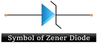
Its symbol is somewhat similar to the symbol of a normal diode. However, a small variation is seen in the symbol of a zener diode which is shown by the bends at the two ends of the vertical line.
Construction of Zener diode
The figure below, represents the diffused structure of a Zener diode:
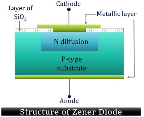
Here, N and P substrate are diffused together. The junction region is covered with a layer of silicon dioxide (SiO2). At the same time during construction, the whole assembly is metallised in order to generate anode and cathode connection. The layer of SiO2 helps to prevent contamination of the junctions. Thus, is used in the construction of zener diode.
Working of Zener diode
The operation of a zener diode is like a normal diode in forward biased mode. That means a large majority current flows through the device when the forward potential is applied to it. However, a zener shows variation from a normal diode in the aspect of its doping concentration. Zener diode is highly doped thus its depletion width is very thin. Due to this, more current flows through a zener diode as compared to a normal junction diode.
It specifically acts in the breakdown region in the reverse biased condition. A zener diode shows two breakdown approach, zener breakdown, and avalanche breakdown.
Let us separately understand the two breakdown mechanism.
- Avalanche breakdown mechanism
Avalanche breakdown is usually subjected to happen when the applied reverse bias voltage is high. As we already know that in reverse biased condition, small minority current flows through a normal diode. When a high reverse biased voltage is applied to the device, the minority carriers experience acceleration and moves with high velocity. During its movement, minority carriers collide with the atoms and generate more number of free electrons. These free electrons further generate some more free electrons. Thus, a high electric current is generated due to this multiplicative action.
Hence, we say high potential in reverse bias is required in case of avalanche breakdown. This high current is responsible for the permanent destruction of a normal diode. But an avalanche diode carefully manufactured to operate in breakdown region withstand the high current flowing through it.
- Zener breakdown mechanism
This breakdown mechanism is noticed in diodes that are heavily doped. Due to the high concentration of impurities, the width of the depletion width is narrow. With the increase in reverse potential, a strong electric field is generated by the depletion region.
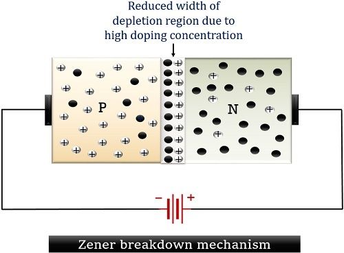
As the reverse potential is supplied to the device and the voltage reaches near to zener voltage. The electrons present in the depletion region utilize that energy and get separated with the parent atom. Thereby generating free electrons. This action generates more free electrons and hence their movement produces electric current through the device. Thus, a small increase in reverse voltage will cause an immediate increase in current through the device. The current flowing through the device shows its maximal increase up to circuit permissible value. This reverse current will remain constant for a wide range of reverse potential.
When a zener diode operates in the breakdown region, it does not burn rapidly. However, the reason for this is some external circuit is required in order to protect the device from the excess current.
VI Characteristics of Zener Diode
The figure below shows the characteristic curve of a zener diode:
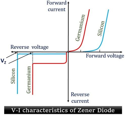
The figure represents the curve for both silicon and germanium diodes. The forward characteristic of the zener diode is similar to a normal diode which is clearly seen in the figure above.
In reverse biased condition, a small reverse current flows due to minority charge carriers. On increasing the reverse voltage, current increases. A point is reached when the junction gets destroyed and a sharp increase in current is noticed without any noticeable increase in reverse potential. This voltage is known as zener voltage. The current through the device is limited by making use of external resistance.
Applications of Zener Diode
Among numerous uses, let us discuss some crucial applications of zener diode:
- In voltage regulation: Regulating the voltage of a circuit is its ability to keep the output voltage fixed regardless of the variation in input voltage or load current.
The figure below represents the circuit of zener diode as voltage regulator:
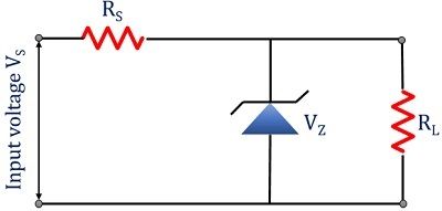
Here, RS is the current limiting resistor, VS is the voltage source and RL represents the load resistance. RS absorbs the voltage fluctuations so as to give a constant voltage at the output. Until load voltage is less than the breakdown voltage, the zener diode does not show conduction.
As the voltage at the load increases than breakdown voltage, the device now starts conduction in the breakdown region. Thus, at the breakdown region, a constant voltage is maintained - In switching operation: A zener diode can be used for switching purpose because it shows an abrupt transition from low to high current. Due to its such switching characteristics, it is widely used in computer applications.
- In meter protection: A zener diode can protect a meter from the excessive voltage applied to it. A parallel connection of zener with the meter causes excess current to pass through zener rather than a meter. Thereby protecting it from severe damage.
- In clipping circuits: Zener finds its applications in the clipping circuit, where the peak of the applied input is clipped off. Usually, clipping is done to protect the voltage sensitive devices from overvoltages.
Key terms related to Zener Diode
Zener voltage: It is that reverse bias voltage at the which junction breakdown completely and large current flows through the device at a constant potential.
Reverse saturation current: It is the current flowing through the device at reverse biased condition due to the flow of minority charge carriers.
Zener impedance: Zener impedance is basically termed as the dynamic resistance of the zener diode. It is defined as the ratio of small change in zener voltage and current.
It is given by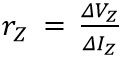
So, we can conclude that a zener diode is definitely a reverse bias device. As it resembles a normal diode in the forward biased region. It is a heavily doped diode, due to which conductivity increases and breakdown is achieved at low voltage.
You have given information about Zener diode in more convincing words, thanks a lot.