DAC is an acronym used for Digital to Analog Converter and DAC interface is used to generate analog output by converting the digital signal obtained from the microprocessor into equivalent analog form. More simply, DACs are devices that perform digital to analog conversion however, this conversion requires a reference value on the basis of which the conversion takes place.
Sometimes there are internal references but all DACs do not have internal references thus in some cases power supply is used as a reference.
Content: DAC Interface
Introduction
In general, it is known that a microprocessor generates only digital signal i.e., in the form of binary values as its output. However, in some applications like in order to control analog devices, analog signals are needed. Due to this reason, DAC interfacing is necessary as using a DAC the digital output of the microprocessor can be converted into analog form.
The input at the DAC unit is binary data which converts it into equivalent analog voltage or current. Every DAC contains ‘n’ number of input lines while a single output line. As we have discussed that a reference value is required therefore, for the operation to take place DAC needs either a reference analog voltage (Vref) or reference analog current (Iref). A word resolution is used to describe the smallest analog value that an n-bit binary code can represent. For the n-bit binary value, DAC resolution is given as 1/2n of the reference analog value. It is to be noted here that every analog output will be a multiple of the resolution.
Suppose if there is an 8-bit DAC where the reference voltage is considered to be 5V then the DAC resolution will be given as:
![]()
This simply means that a digital input of 8-bit value can provide 28 i.e., 256 different values.
Mainly the DAC is classified into 3 categories:
- Current Output DAC
- Voltage Output DAC
- Multiplying type DAC
As the name indicates the current and voltage output DACs are the ones that generate analog current and voltage signal respectively as its output. The operation of voltage output DAC is such that internally the analog current signal is transformed into voltage equivalent. Other than these two types the third one is the multiplying type DAC that provides the output which is the product of applied input and the reference source. Though the difference is simple, even current output DAC and voltage output DAC can be considered as multiplying type DAC as all of them provide such an output which is the product of applied input with the reference value.
Digital to Analog Converter
The figure below represents the DAC network consisting of the resistive ladder:
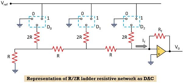
Here we are having a resistive network of adequate values along with switches and reference sources.
The above arrangement contains switches and the switches can be transistors connected with the resistance which forms a connection either with the ground or the reference voltage. The connection of the resistors in the circuit is done in such a way that the overall current of the circuit appears in binary proportion. The network contains an op-amp that provides a voltage signal as output from the obtained current signal.
The obtained output voltage for the above network will be given as:
![]()
In case, if we consider 8-bit DAC then a number of R/2R ladder in the network will get increased thus the modified equation for output voltage will be:
![]()
The time duration in which a digital signal is converted into an analog one is known as conversion time. This conversion time shows dependency on the response time of switching transistors along with the characteristics of the output amplifier.
It is to be noted here that at the time of interfacing the DAC with the microprocessor the digital signal must be present at the input of the DAC continuously till the time of completion of the ongoing conversion process. This means holding the data at the input is necessary and for this latch is used at the input of the DAC.
One of the examples of DAC is AD558 that is an 8-bit DAC with an internal latch and I to V converting amplifier. This DAC provides an analog voltage signal as its output. This DAC can be directly interfaced with the 8085/8086 microprocessor using two control signals namely Chip Select and Chip Enable. Other than this DAC0800 is another example of an 8-bit DAC however this does not operate without an internal latch and I to V converting amplifier. Its interfacing can be done using a port device or latch.
DAC0800
The figure given below represents the block diagram representation of DAC0800:
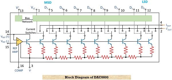
It is an 8-bit DAC that offers high speed and is a current output type of DAC that means it provides analog current as its output. The conversion time offered by this DAC is around 100 ns. The current output signal obtained from it can be converted into voltage by making use of a resistor.
The input supply provided to it is in the range of ± 5 V to ± 18 V. This can be directly interfaced with TTL or any other logic family member. The value of the analog current obtained at the output depends on the applied digital input as well as the reference voltage value. This analog current can be converted into analog voltage by the use of a resistor across the output terminal.
Here we have shown the pin diagram of DAC0800 DIP 16-pin arrangement:
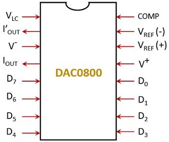
As it is an 8-bit DAC thus it contains 8 digital input lines. Other than the input lines we have two dedicated pins that provide current output and complement of current output which is given the name IOUT and I’OUT. There are a positive and a negative supply voltage pin along with a pin dedicated for compensation voltage. Here VLC represents the threshold control pin and there are two pins for positive and negative values of reference voltage denoted by VREF (+) and VREF (-).
Interfacing DAC0800 with 8085 Microprocessor
Basically, latch (8-bit) is used to interface DAC0800 to an 8085 based system bus, and in order to enable these latch chip select signals are used that are generated by IO devices. The figure below shows the interfacing of DAC0800 with 8085:
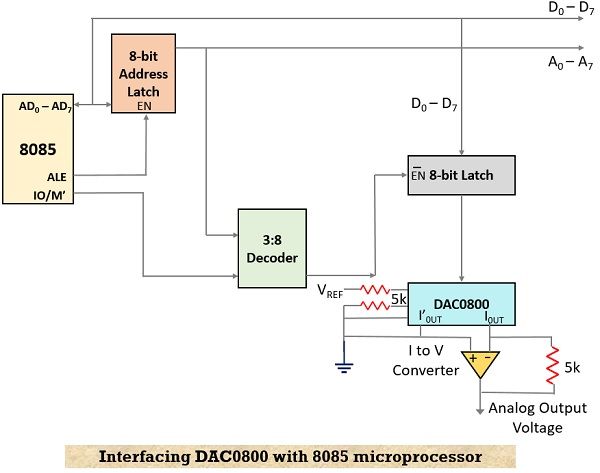
The latch used for the purpose of interfacing here is 74LS273 it is a 3-to-8 decoder that generates the chip select signals for the associated input-output devices.
Here digital data is changed into analog output, the processor first loads the data onto the latch and the latch will hold the previous data till the time the previous operation is taking place. Once the previous operation has been completed then the next data will get loaded. A definite amount of time is needed by the DAC in order to change the digital data into analog one. This means that the successive data will get loaded into the latch only when conversion time has been completed.