Programmable interrupt controllers are used to enhance the number of interrupts of a microprocessor. 8259 is a programmable interrupt controller which shows compatibility with 8085 microprocessor.
It is also known as a priority interrupt controller and was designed by Intel to increase the interrupt handling ability of the microprocessor. An 8259 PIC never services an interrupt; it simply forwards the interrupt to the processor for the execution of interrupt service routine.
Content: 8259 Programmable Interrupt Controller
Need of Programmable Interrupt Controller
We know whenever an interrupt occurs then the microprocessor suspends the current program and switches to the Interrupt Service Routine (ISR).
We know 8085 has 5 interrupts, which are: Trap, RST7.5, RST6.5, RST5.5 and INTR.
Among all these, only INTR is a non-vectored type of interrupt, rest are vectored interrupts.
We know vectored interrupts are those interrupts whose ISR address is known to the processor. Or we can say in case of vectored interrupts, the processor holds the address of the memory location where ISR is stored.
But in case of non-vectored interrupts, the processor has to reach the ISR but it does not hold the address of ISR. So, in this case, the interrupt generating device provides the ISR address to the microprocessor.
An 8085 has 5 major interrupts for which a fixed number of lines are present in the chip. But there are many devices connected to a processor. So, for such a case the processor must have more number of lines to handle several interrupts.
But it is not practically possible to increase the number of lines each time with the increase in the number of interrupts.
So, to overcome this problem 8259 PIC chip is used. 8259 allows the combining of multiple interrupts and providing them to the processor based on priority through a common line.
As we have already discussed that the processor holds the address of ISR in case of vectored interrupts. So, it is not possible to combine a non-vectored interrupt with a vectored one.
Therefore, 8259 is used to combine various interrupts which are non-vectored in nature.
Also, suppose in some way or the other, two devices generate interrupt simultaneously through a common line without the involvement of 8259.
So, the processor gets two INTR signals at the same time but how does the processor get to know that from where the interrupt is generating and where to send the INTA in order to have the ISR address.
This shows the necessity of 8259. The programmable interrupt controller tells the microprocessor about the interrupt. Basically the external devices initially interrupt the 8259 and further the 8259 interrupts the microprocessor.
Features of 8259
- The 8259 programmable interrupt controller has 8 interrupt pins thus can handle 8 interrupt inputs.
- The priority of interrupts in 8259 can be programmed. The priority of interrupts is decided by the different operating modes.
- We know that a single 8259 can handle 8 interrupt inputs but by cascading multiple 8259, it can handle maximal 64 interrupt inputs.
- 8259 allows individual masking of each generated interrupt using interrupt mask register.
- 8259 is programmed in a way that it can handle either edge-triggered or level-triggered interrupt request at a time.
- If multiple interrupts are generated, then 8259 holds the status of interrupts that are masked, in-service and pending.
- It reduces the software and real-time overhead generated due to handling multilevel priority interrupts.
Architecture of 8259
The figure below shows the architectural representation of 8259 programmable interrupt controller:
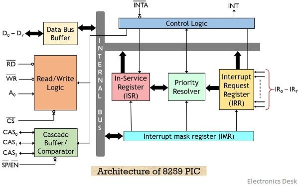
It has an 8-bit of data bus. As we have already discussed that 8259 never services the interrupt, it simply forwards the interrupts to the microprocessor.
Thus, the above architecture has different units that combinely functions to increase the interrupts handled by the processor.
Let us understand the operation performed by each unit in detail:
1. Data Bus Buffer: 8259 has tri-stated bidirectional 8-bit data bus buffer (i.e., D0 to D7) that interfaces with the internal bus of the processor. The 8085 microprocessor sends/ receives, control or status words to/ from the 8259 using data bus buffer.
2. Read/ Write Logic: This unit is responsible for controlling the internal read-write operations of the system. It holds initialization command word register and operation command word register inside which various control formats exist that are needed for the device operation.
RD, WR, A0 and CS are the pins that are associated with this unit. Basically, these pins are used by the processor for read and write operations.
A low signal at CS i.e., chip select shows that now the communication has been set up between the processor and 8259.
3. Control Logic: This unit is the heart of the architecture of 8259. It controls the overall operation of the system by sending the INTR signal to the processor whenever an interrupt request is generated.
Also, it receives INTA signal by the processor when microprocessor demands for the address of the interrupt service routine. The control logic is responsible for sending the address of the desired interrupt service routine through the data bus.
4. Interrupt request register (IRR): This unit stores the interrupt requests generated by the peripheral devices. We know that 8259 has 8 interrupt request pins (i.e., IR0 to IR7). So, the unit can store 8 interrupt requests that are requesting the service from the processor.
5. Priority Resolver: This logic unit decides that among all the interrupt request present in the IRR which holds the highest priority and needs to be executed first.
Suppose at the time of servicing an interrupt, another incoming interrupt request gets generated then that request will be ignored as the one in-service is holding the highest priority.
But in case the incoming request has greater priority than the one which is being in current execution then that respective bit will be set in ISR and INTR signal is sent to the microprocessor.
This simply means that only the interrupt holding the highest priority will be forwarded by the 8259 to the processor.
6. In-service register: Here the name of the unit is itself indicating the operation performed by it. This register unit stores the interrupts which are currently being executed by the processor.
The priority resolver sets each bit of ISR and after getting interrupt word command by the processor, the bits get reset. As the processor holds the ability to directly read the status of in-service register.
7. Interrupt mask register: This register unit holds the masking bit of those interrupts which are to be masked. Through operation command word (OCW) the processor sends the required information and programs the interrupt mask register.
8. Cascade buffer/comparator: As we have already discussed that by cascading multiple 8259, the number of interrupts handled by 8259 can be expanded up to 64. The unit allows the comparison of IDs of different 8259s cascaded together.
It permits the operation of the system in two modes: master mode and slave mode.
In the master mode of operation, it acts as a cascaded buffer. Whereas in slave mode, this unit acts as a comparator.
Among the various cascaded 8259, one 8259 directly handles the interrupts by forming a connection with the processor and it is known to be master 8259. While the other 8259s that interrupts the master 8259 are known as slave 8259.
Each of the 8259s can be separately programmed as all of them holds a specific address. The cascading pins of the master 8259, CAS0, CAS1 and CAS2 forms connection with the corresponding pins of slave 8259s.
For the slave devices, these pins act as input pins while for a master device these acts as output pins. An active-low signal at SP/EN for a device shows that it is operating in slave mode.
In this way, a programmable interrupt controller operates.