8251 USART is a universal synchronous and asynchronous controller designed by Intel basically to facilitate communication.
USART stands for Universal Synchronous and Asynchronous Receiver Transmitter and functions as an intermediary that allows serial and parallel communication between the microprocessor and the peripheral devices.
We know that microprocessors allow parallel communication. And in parallel communication, the number of cables required for data transmission is equal to the number of bits to be transmitted per cycle.
Thus the approach of transmitting data parallelly to long distance is cost-ineffective.
So, to reduce the overall cost of the system despite parallel data communication between the processor and peripheral devices, the serial transfer of data is permitted.
Hence for this purpose, USART acts as a mediator between the processor and peripheral devices so, that the parallel data from the processor can be converted into serial data and efficiently transferred to the peripheral devices.
In a similar way, the serial data from the peripheral devices is converted by the USART into the parallel form so that it can be accepted by the processor.
Also, it allows both synchronous and asynchronous transmission and reception thus is called so.
Architecture and Working of 8251 USART
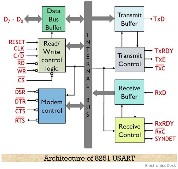
The figure below shows the architectural representation of 8251:
 Let us now understand the operation performed by each unit in detail:
1. Data Bus Buffer: It basically interfaces the 8251 with the internal system buses of the processor.
The data bus buffer has 8-bit bidirectional data bus that allows the transfer of data bytes, status or command word between the processor and external devices.
2. Read/Write Control Logic: This functional unit generates a control signal for the operation of 8251 according to the signal present in the control bus of the processor. Basically, it performs decoding operation of the control signal produced by the processor, so that respective operation can be performed by the USART.
The control formats for system operation is stored in control and command word registers present in the read/write logic unit.
The signals handled by the read/write control logic unit are discussed below:
- CS: It is chip select. A low signal at this pin shows that processor has selected 8251 in order to communicate with the peripheral devices.
- C/D: As the system has control, status and data register. So, when a high signal is present at this pin then control or status register is addressed. While in case of low signal data register is addressed.
- RD and WR: Both read and write are active low signal pins. A low signal at RD shows that the processor is reading the control, status or data bytes from the 8251. While at WR indicates the write operation over the data bus of 8251.
- CLK and RESET: CLK stands for clock and it produces the internal timing for the device. While an active high signal at the RESET pin puts the 8251 in the idle mode.
3. Transmit Buffer: This unit is used to change the parallel data received from the CPU into serial data by inserting the necessary framing information. Once the data is transformed into serial form, then in order to transmit it to the external devices, it is provided to the TxD pin of the 8251.
This unit consists of 2 registers. These are as follows:
- Buffer register: Basically the data provided by the processor is stored in the buffer register. As we know that initially, the CPU provides parallel data to 8251. So, the processor loads the parallel data to the buffer register. Further, this data is fed to the output register.
- Output register: The parallel data from the buffer register is fed to the empty output register.
This register changes the 8-bit parallel data into a stream of serial bits. Then further the serial data is provided at the TxD pin so as to have its transfer to the peripheral device.
As we have already discussed that it performs both synchronous and asynchronous transmission and reception. Thus in case of asynchronous transmission, start and stop bit is added by the transmitter in order to notify the external devices about the data transmission.
But in case of synchronous transmission, the clock signal is used thus there exists no need of adding additional bits expect the parity bit (if required).
4. Transmit Control: As the name of the unit is itself indicating that it is controlling the transmission action. And it does so by accepting and sending signals both externally and internally.
The various control signal generated by this unit are as given below:
- TxRDY: It implies transmit ready. This signal is used to notify the processor that the buffer register of the 8251 is empty and ready to accept the data.
The status read operation is utilized by the processor in order to check the presence of the signal. - TxE: This stands for transmitter empty. It is an active high signal that indicates that the output buffer is empty and thus data received from the processor can be loaded to it for conversion.
- TxC: It stands for transmitter clock and is an active low pin. It controls the rate of character transmission by the USART.
However, 8251 offers programmable clock rate. As by writing appropriate mode word in the mode set register the clock division can be programmed.
5. Receive Buffer: This unit takes the serial data from the external devices, changes the serial data into the parallel form so that it can be accepted by the processor. It consists of 2 registers: receiver input register and buffer register.
When the external device is ready to send the data to the 8251 then it sends a low signal to the RxD line of the 8251. In asynchronous mode, once 8251 receives a low signal it considers that signal as start bit of the data.
So, once the start bit is successfully accepted by 8251, then it also receives the whole data bits in serial form along with parity and stop bits.
Once the data is received by the receiver input register then it converts the data bits in parallel form and sends it to the receiver buffer register.
In case of the synchronous mode of operation, according to the clock input, the external device loads the serial data bits in the receiver input register. And on converting the serial data to parallel format the receiver input register sends the data to the buffer register.
6. Receiver Control
This unit controls the operation of the receiver buffer. It manages the data reception, along with that it also detects the presence of false start bit, error in parity bit, framing errors etc.
- RxRDY: It stands for receiver ready. When this signal goes high then it indicates that the receiver buffer register is holding the data and is ready to transfer it to the processor. Once the CPU reads the data sent by the 8251 then this pin is reset.
- RxC: It stands for receiver clock. This clock signalling controls the rate at which the 8251 receives the data in the synchronous mode of operation. It is provided by the modem and is equal to the baud rate.
While asynchronous mode offers the clock rate as 1, 16 or 64 times of the baud rate as it is programmable.
7. Modem Control: This unit of 8251 holds input and output control signals that simplify the operation of the whole system. The control circuitry for handing various signals is provided by the modem control unit. It includes DTS, RTS, DTR and CTS.
These are all active low signals.
- DSR: Stands for data set ready and the signal is used to check whether the data set is ready or not when the processor is in the urge of communication.
- DTR: Implies data terminal ready. An active-low signal at this pin shows that the 8251 is now ready to accept the data from the processor.
- RTS: It stands for the request to send. A low signal shows an assertion for data transmission.
- CTS: Clear to send. When 8251 receives a low signal at this pin then it clears all the data present in the modem in order to allow further communication.
This is all about the architectural working of 8251 USART.
Very Nice information about working of 8251 USART.
Good information about 8251.