Definition: A Gunn diode is a semiconductor device formed by only N-type material. It is also termed as a transferred electron device. As in n-type material, electrons acts as majority carriers and these are transferred from one valley to another.
It is a two terminal device basically made up of semiconductor material like GaAs, InP etc. As these materials exhibit the property of producing microwave oscillations.
Gunn effect is the basis of working of Gunn diode. It was discovered by a physicist J B Gunn in 1963.
A Gunn diode does not contain a pn junction yet it is termed as diode due to the two terminals of the externally applied dc voltage. It possesses negative resistance characteristic due to which these are widely used in high-frequency applications.
Gunn diodes have the ability to generate continuous power in the range of several milliwatts, and frequency nearly 1 to 200 GHz holding efficiency about 5 to 15%.
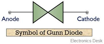
The figure below shows the symbolic representation of Gunn diode:
What is Gunn Effect?
In semiconductor materials like GaAs, the electrons are present in high mass low-velocity state and low mass but a high-velocity state. By the application of sufficient electric field, these low mass high-velocity state electrons are forced towards the high mass state.
At this particular state, electrons form a cluster and thus moves at a uniform rate. Thus causing a flow of current in the form of a series of pulses.
This is termed as Gunn effect and is utilized by Gunn diodes, hence, named so.
Construction of Gunn diode
We have already discussed that a Gunn diode is not a pn junction diode as it is composed of only n-type semiconductor material. The figure below represents the constructional structure of a Gunn diode:
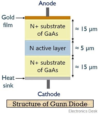
Here, a lightly doped n-type semiconductor layer is present between two heavily doped n-type material. The middle portion is termed as an active layer. The thickness of this region is around a few microns to several hundred microns.
The arrangement of Gunn diode is formed by growing an epitaxial n-type layer over an n+ substrate. The 2 highly doped regions provide better conductivity to the device.
The whole structure is mounted on a conducting base that acts as a heat sink for the heat produced during operation. Also, the other terminal is formed by connecting a gold film over the top surface of the structure.
Working of Gunn Diode
The operation of Gunn diode depends on Gunn effect which we have already discussed in the previous section of this article. So, now let us have a look at how a Gunn diode actually operates.
When a voltage is applied to the device, then this external potential appears across the active layer thereby causing the flow of electrons present in that region. This flow of majority carriers causes the current to flow across the active region of the device.
Once the current pulse starts traversing inside the active region, the potential at that region falls. Due to which no further formation of the current pulse occurs.
But once the previously created current pulse reaches the other end of the active region then the potential again rises leading to the generation of another current pulse.
Thus, the frequency of operation of the device depends on the time taken by the pulse to travel to another end, resultantly on the rate of pulse generation.
Unlike a normal junction diode, a Gunn diode consists of 3 energy bands namely, valence band, conduction band and an extra band above the conduction band.
The figure below represents the energy level structure of the gallium arsenide:
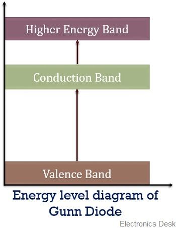
When a certain voltage is applied to the device then electrons in the valence band starts moving towards the conduction band thereby allowing the flow of current.
But when the voltage further increases then instead of allowing a large flow of current the electrons in the conduction band move towards the energy band present above the conduction band.
Due to this the effect is known as the transferred electron effect. This is so because electrons are transferred from conduction band to a higher energy state.
At this particular state as the electrons are less mobile hence current decreases with the increase in voltage. Thereby, giving rise to a negative resistance phenomenon where current decreases with the increase in voltage.
After a certain point of time when the applied voltage increases further then the electrons in the higher energy state gains sufficient energy and moves back to the lower energy state. Thus, further the current flowing through the device increase with the increase in the applied external potential.
Characteristic curve of Gunn Diode
The figure below shows the characteristic curve of a Gunn diode:
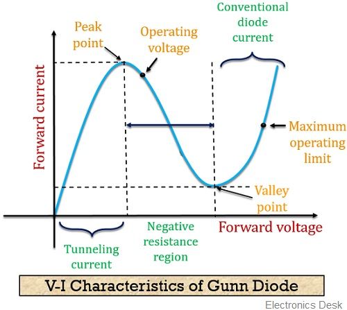
Here, we can clearly relate the above explanation with the curve shown. Initially, with the increase in the applied voltage, the current through the device also increases.
However, a point is reached when on increasing the voltage the current through the device starts decreasing. The point of maximum current is known as the peak point.
The region on the curve that shows the decrease in current with an increase in voltage is known as the negative resistance region of the curve.
The negative resistance characteristic is also exhibited by a tunnel diode but the two show variation in their operating manner.
Advantages of Gunn Diode
- The manufacturing cost of gunn diode is low.
- Gunn diodes are highly reliable.
- It exhibits comparatively low operating voltage than normal diodes.
- Its installation in circuits is easy.
Disadvantages of Gunn Diode
- These are less stable.
- The efficiency of gunn diodes is very low.
- Sometimes noise effects are more in case of gunn diodes.
Applications of Gunn Diodes
Gunn diodes find their applications in oscillators and amplifiers, in ultrasonic detectors. These are also used in tachometers and in the radio communication system.