Definition: A heavily doped two-terminal semiconductor device through which electric current flows because of tunneling ( or tunnelling) of electrons is known as Tunnel Diode. It possesses the negative resistance characteristic in which current decreases even when the applied voltage is increased.
Tunneling basically denotes the penetration of electrons through the depletion region. As highly doped diode has a thin depletion region. It works on the principle of Quantum mechanical tunneling. As tunnel diodes show fast switching characteristics thus it finds extensive applications in the field of the microwave.
Content: Tunnel Diode
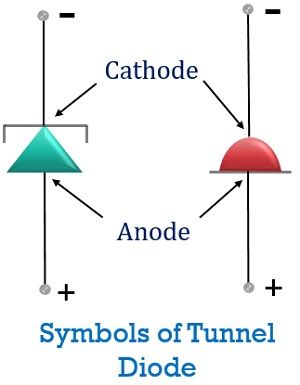
Symbol of Tunnel diode
The symbolic representation of tunnel diode is shown below:
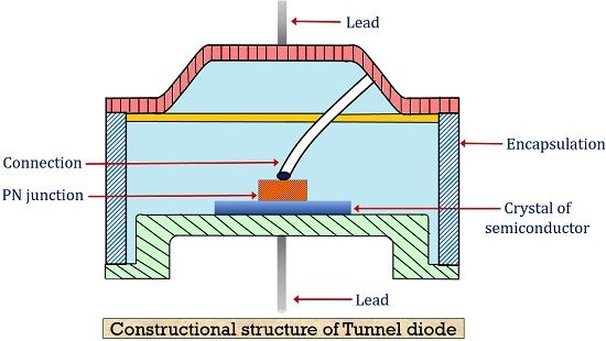
Construction of Tunnel Diode
The basic manufacturing material of a tunnel diode is germanium, gallium arsenide or gallium antimonide. It is not formed using silicon as its basic material. This is so because the ratio of maximal value of forward current to valley current in case of silicon is very low. However, gallium arsenide has the maximum value of this ratio thus is widely used.
The structural representation of tunnel diode is shown below:
In the tunnel diode, the doping concentration is very high. The concentration of doped impurity in a tunnel diode is thousand times more as compared to any normal diode. This is done so as to have thin depletion region, that is the basis of tunneling effect.
This diode was invented by Dr Leo Esaki in 1957. Hence it is also known as Esaki Diode.
Working principle of Tunnel Diode
As we have already discussed that the doping concentration in case of tunnel diode is very high. Due to this, the reduced width of the depletion region causes the penetration of charge carriers across the junction even when the carriers do not have enough energy to jump across it.
Let us understand the working of a tunnel diode by considering some conditions.
- In a zero biased condition, the highly doped diode is not provided with any input voltage. So, in no biased condition, an overlapping is noticed between the conduction band of n region and valence band of p region.
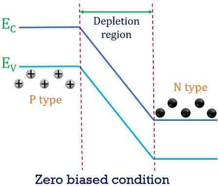
This overlapping causes the two bands to appear at the almost same energy level. As the depletion width is very small thus, without any applied potential, due to temperature variation, electrons from n side tunnels to p side.
Similarly, holes from p side tunnels to n side.
As the tunneling is equal for both the carriers thus no current is noticed in case of zero biased condition. - Now, when a certain forward voltage is applied to the diode, no any current will flow due to this applied potential. As this forward voltage is less than the barrier potential of the depletion region.
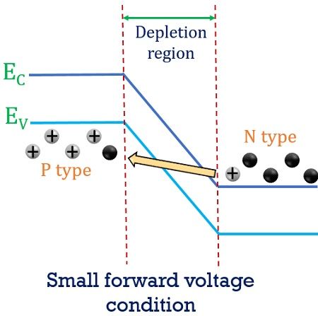
But, still, a small current flows through the device. This is so, because, the electrons in the conduction band of n region will penetrate over thin depletion region and reaches valence band of p region.
The velocity of punching of these electrons is somewhat similar to the velocity of light. Hence, this punching generates a forward current through the device. - Now, when the applied forward voltage is increased further. So, in this case, a large current starts to flow through the device. The electrons that have sufficient energy moves across the junction. But those which has less energy will also penetrate the junction due to thin depletion width.
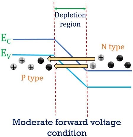
In this case, more electrons tunnel through the junction to reach p region. This is so because now, the conduction band of n region is parallel with the valence band of p region. Thus, the highest (peak) current is achieved in this condition. - If the forward potential applied to the device is increased further. Then the conduction band and valence band shows some overlapping. This causes a small current to flow through the device. However, here with the increased potential current through the device now starts decreasing.
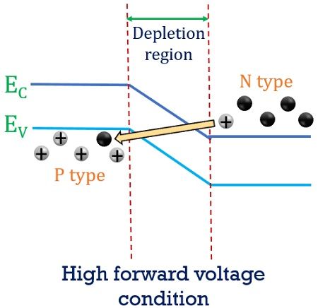
After this, the applied potential is increased further. But now this applied voltage will cause the current through the device to reach nearly zero. As the conduction and valence are no longer forming an overlap connection. But, the applied potential will now overcome the barrier potential of the depletion region. So, current as in case of the normal diode will flow through the tunnel diode also.
This is how a tunnel diode works.
Characteristics of Tunnel Diode
The figure below represents the VI characteristics of a tunnel diode:
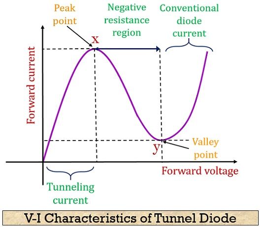
Here we can see the origin of the graph shows the zero biased condition of the tunnel diode. Where no any input voltage is provided and so no current is noticed in the device. As the input voltage is increased, the current is noticed to flow through the device. This current increases with the increase in the voltage applied and a peak of forward current is reached. This is clearly represented by point x in the above figure.
As we discussed already that after reaching the maximum value, the current now starts decreasing. This region of the decrease in current in the graph is specifically termed as a negative resistance region. After this region valley point is achieved which shows the decrement of the current nearly up to zero.
But, as the potential has increased the device now starts behaving as normal junction diode. Thus, the current begins to increase from this particular point.
Advantages of Tunnel Diode
- It is a low power consuming device.
- It is not expensive.
- A tunnel diode is easy to operate and provides high-speed operation.
Disadvantages of Tunnel Diode
- The abrupt change in load current with applied voltage is sometimes treated as its drawback.
- Proper isolation between input and output is not maintained as it is a two terminal device.
Applications of Tunnel Diode
It is widely used in microwave and high-frequency applications because of its fast response. It can be also used as amplifiers and in oscillator circuits.
Key terms related to Tunnel Diode
Tunneling current: It is the current flowing through the device due to the punching of electrons across the junction. The thin depletion width allows some free electrons to tunnel the junction rather than jumping over it. This penetration of electrons generates a current known as Tunneling current.
Negative resistance characteristics: The negative resistance characteristic is the special ability of tunnel diode in which current represents fall even when the voltage provided to it rises.
Valley current: When tunneling reaches its minimum value with the increase in forward potential. Then the lowest value of tunneling current is the valley point of the device.
So, we can conclude that the device possesses conduction initially due to quantum mechanics. After reaching some specified large forward potential the tunnel diode begins to behave like a normal diode.
Very nice explanation