Definition: An electronic component made of semiconductor material that allows conduction of current in only one direction is termed as a Diode. It is a two-terminal device normally formed by fusing p and n-type semiconductor materials each having majority and minority carriers.
Let us first see the major contents of this article.
Content: Diode
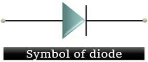
Symbol of Diode
The figure below shows the symbol of the PN junction diode:
Construction of a Diode
After having a basic definition, let us now proceed towards the formation.
A diode in its fundamental form is a PN junction device through which current flows when the proper forward potential is applied. The p and n-type semiconductor materials must be carefully combined so that the two must have a controlled quantity of donor and acceptor impurities. In its basic form, a single silicon or germanium wafer is taken which is doped with pentavalent and trivalent impurities in its two halves. P region denotes the doping of trivalent impurity and n region denotes the doping of pentavalent impurity. Or simply, we can merge separate p and n-type material in order to form the semiconductor device.
The figure given below shows the structure of a PN junction diode:
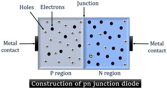
Here, as we can see a p-type semiconductor material is merged with an n-type semiconductor material that forms a junction. This junction is known as PN junction. At the opposite ends, two metal contacts are attached that combinedly form PN junction diode. The p-type material holds holes as its majority carrier and electrons as its minority carrier. As against, the n-type material has electrons as its majority carrier and holes as its minority carrier.
This p-n junction is nothing but a layer of immobile ions termed as depletion layer. When a proper potential is provided then conducting and non-conducting state is noticed in it.
Working of Diode
The operation of a diode involves unbiased, forward biased, and reverse biased condition.
We will discuss the above-mentioned condition in detail. Let us start with the unbiased condition.
- The unbiased condition of a diode:
When no any external potential or voltage is provided to the device. Then it is known as the unbiased condition of a diode.
The figure given below will help you to have a better understanding of the unbiased condition of a diode.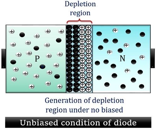
Here, the p-type material is fused with an n-type material. This fusion creates a junction. When no voltage is applied across the diode then, majority charge carriers i.e., holes from p side and electrons from n side get combined with each other at the junction. These charge carriers on combining generate immobile ions that deplete across the junction. Due to this a depletion region is formed at the junction.
It is to be noted here that the flow of charge carriers across the cross-section area is known as diffusion. Hence the current at no bias condition is known as diffusion current.
The potential difference at the depletion region generates an electric field across it. Due to this electric field no any further movement of majority charge carriers is allowed. This is why the width of the depletion region is fixed. The potential at the depletion region acts as a barrier for further movement hence known as a barrier or built-in potential. However, still, minority carrier drifts across the depletion region and a negligible current flows. This very small current due to minority carriers is known as drift current.
- The forward biased condition of a diode:
In the forward biased condition, p side of the device is connected with the positive terminal of the supply. And n side is connected with the negative battery potential. Thereby causing the junction to be forward biased.
Below a figure is given that represents the diode arrangement with positive biasing:
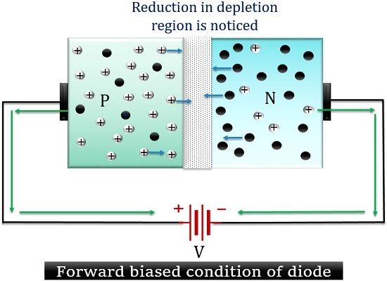
When forward biasing is applied. The holes in the p side experience a repulsive force from the positive terminal. Similarly, electrons experience a repulsion from the negative terminal of the supply provided. However, initially, the majority carriers from both the sides do not move across the junction due to barrier potential.
But, as the barrier potential is exceeded, the majority charge carrier now shows movement across the junction. This movement of charge carriers after overcoming the barrier potential generates current. This current is known as the majority current. The moment this barrier is removed, the resistance offered by the junction becomes automatically 0. Thus, a forward current now starts to flow through the device.
It is noteworthy here that the barrier potential offered by silicon is 0.7V and for germanium is 0.3V. So, after overcoming the respective potential in case of both the materials, forward current starts flowing through the device.
- The reverse biased condition of Diode:
When we externally provide the potential to the device in such a way that p side is connected to the negative terminal of the supply. And n side is connected with the positive terminal. Then the device is said to be reverse biased.
The figure below shows the reverse-biased arrangement of a PN junction diode:
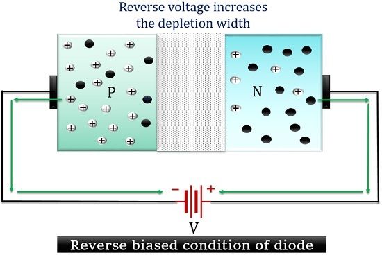
When a reverse potential is applied the holes from the p side experience attraction from the negative terminal. And electrons in n side experiences attraction from the positive terminal of the supply provided. Due to this, the majority carriers present in both the side move in the direction away from the junction. This broadens the width of the depletion region and hence the potential barrier is increased.
This takes the device to a non-conducting state. However, due to the minority carriers present in both p and n side, a very small current flows. This small current through the device is known as reverse leakage current. This reverse current is independent of barrier potential and depends only on the temperature and construction of the device.
Diode current equation
The diode current is given by the following relation:
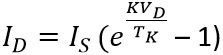
: ID = diode current
IS = reverse saturation current
VD = voltage across the device
TK = temperature in Kelvin
K = 11600/ƞ
ƞ = ideality factor ranges between 1 and 2
Since,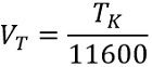
We can also write,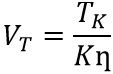
Or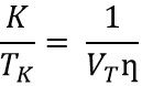
Thus, on substituting the above value in the basic equation. We get,
This is the simplified diode current equation.
Characteristic Curve of a Diode
The figure given below shows the characteristic curve of a PN junction diode in forward and reverse biased condition:
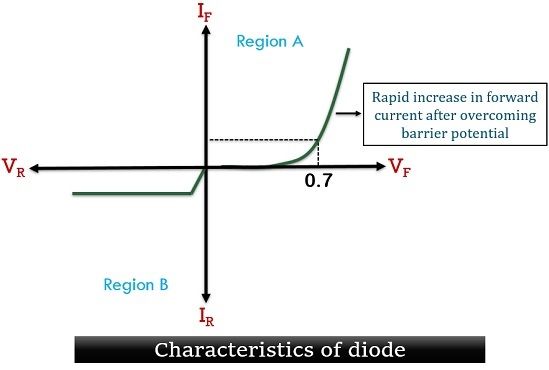
Region A represents the curve for the forward-biased diode. While region B shows a curve for the reverse-biased diode.
Let us consider that diode is made of silicon material. Hence external potential required to overcome barrier potential is 0.7V in its case. Thus we can see in forward biased region, a rapid increase in current is noticed after 0.7 volts. This is known as knee voltage after which barrier potential is totally removed and the device starts conduction.
Now, coming towards region B that represents the reverse biased condition of the device. As we have already discussed that in a reverse biased case, the width of the depletion region is very large and so the barrier potential. Thus the curve represents the reverse saturation current that flows only due to the movement of minority charge carriers through the device. This reverse current is merely less than 1 microamps for a silicon device.
Another noteworthy point here is that, at a nominal reverse voltage, a small reverse current flows. But, on increasing the reverse voltage, a condition arises that causes the junction of the diode to get a breakdown. This causes an immediate increase in the reverse current through it.
Types of Diode
These are basically characterized on the basis of their operating principle, providing different terminal characteristics and allowing multiple uses. The various types of diodes are given below:
Zener diode: It is a type of PN junction diode that finds its operation in reverse biased condition. More specifically we can say in the breakdown region.
It is basically a heavily doped PN junction diode and finds its application in voltage regulation, meter protection and in switching and clipping operations.
Tunnel diode: A tunnel diode is also known as the Esaki diode is a densely doped highly conductive device. Its impurity concentration shows variation with normal PN junction diode. It is based on the principle of tunnelling and shows negative resistance characteristics.
As it shows fast response thus widely used as an amplifier and oscillator. As it is a low current device thus not widely used.
PIN diode: It is a 3-layer device in which an intrinsic region is sandwiched between p and an n-type semiconductor. As intrinsic layer provides high resistivity thus provides key to process small input signals.
These are widely used in microwave and radar applications.
Varactor diode: It is also known as varicap diodes which is a word composed of a combination of the variable capacitor. It is a reverse-biased diode whose operating mode depends on transition capacitance. These are widely used in high-frequency applications.
Photodiode: A photodiode is a device that generates current when a proper region is exposed to light. It also operates in a reverse-biased condition. These are widely used in detection, demodulation, switching and encoding applications.
LED: LED is a short form of light-emitting diodes. It is a device that produces incoherent light due to an applied electric field. It is a forward-biased diode. LEDs are widely used in digital watches, in multimeters and burglar alarms etc.
Laser diode: Laser is an abbreviation for light amplification by stimulated emission of radiation. These are specifically designed to produce coherent radiation. Laser diodes are widely used in telecommunications and medical applications.
Schottky diode: It is not a PN junction diode as it is formed by merging metal with the n-type semiconductor material. This eliminates the depletion region. These are widely used in digital computers.
Key terms related to Diode
Barrier potential: It is the voltage generated at the junction under zero biased condition due to immobile ions. Also known as built-in potential.
Knee voltage: It is that forward bias voltage of a semiconductor device that overcomes the barrier potential. After this voltage, a high number of charge carriers move across the junction. Resultantly high current flows through the device. Its value is 0.3V for germanium and 0.7V for silicon.
Breakdown voltage: At reverse bias, a very small current is noticed in the device due to the flow of minority carriers. However, if the reverse voltage is increased beyond a certain limit. Then it causes the junction to break down completely. This voltage is known as the breakdown voltage.
Peak inverse voltage: We can understand peak inverse voltage (PIV) by the name itself. Peak means the highest or maximum and inverse means the reverse. So, it is basically that maximum voltage at a reverse biased condition which can be withstood by the device.
So, we can conclude that the current through a semiconductor diode depends on its biasing arrangement or applied input to it.