Definition: Varactor Diode is a PN junction diode that is especially operated in reverse biased mode. It is a device whose capacitance varies with the variation in the applied reverse bias potential. It is also known as varicap or voltcap. The word varicap is derived from the combination of word variable and capacitor.
As these are specially designed diodes thus exhibits the characteristic of transition capacitance far better as compared to normal PN junction diodes.
Content: Varactor Diode
Symbol of Varactor Diode
The figure below shows the symbolic representation of a varactor diode:
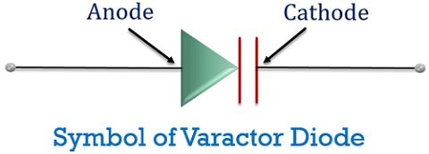
Its symbol is somewhat similar to an ordinary diode. However, in varactor diode, the cathode terminal is shown by the 2 plates of the capacitor. This is done to represent the effect of capacitance during operation.
Construction of Varactor Diode
A varactor diode is formed by merging a p-type semiconductor material with the n-type semiconductor material. According to the use, the p and n regions are made of either silicon or gallium arsenide material. In the case of low-frequency uses, the basic material used is silicon. And in case of use in the high-frequency field, it is fabricated with gallium arsenide.
The figure representing the construction of a varactor diode is shown below:
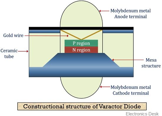
As we can see here that, n region is connected with the mesa structure. Through this mesa structure, a molybdenum metal with gold plating is connected to the n region which serves as a cathode terminal of the whole unit. Similarly, the p region is also connected with the molybdenum metal but this time the connection is through a gold wire. This acts as the anode terminal of the device. A ceramic layer is used to enclose the whole structure of the diode excluding the anode and cathode terminal.
Working of Varactor Diode
As we have already discussed that the varactor diode is a reverse biased device. That means the operation for which it is specified is noticed in a reverse biased condition rather than forward biased. Now, the question arises why this is so?
Let us first understand why it is not operated in forward biased condition.
When a diode is provided forward potential. Then the majority carriers present both in p and n region experiences repulsion from the battery. Due to this, after a certain voltage, the depletion region diminishes and the device starts conducting heavily. But, a varactor diode is basically manufactured to store the charges rather than conducting current. This is the reason why we provide reverse bias to the diode.
Let us move ahead to understand reverse bias operation of varactor diode. The figure below represents the reverse biased arrangement of the varactor diode:
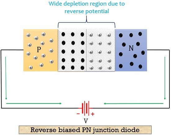
Initially, a thin depletion region is present in case of no bias condition. But as the reverse potential is applied the majority carriers of both the p and n regions i.e., holes and electrons start moving away from the junction. Due to this, the majority carriers depleted from the junction. So, as the reverse potential is increased, the depletion width also increases. In this case, the two regions serve as the capacitor plates and the depletion region behaves as an insulating dielectric.
The capacitance at the junction is termed as transition capacitance. It is designated as CT. As we know the capacitance is given by
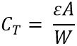
: ε = permittivity of the material
A = area of the junction
W = depletion region width
So, from the above expression it is clear that, with the rise in the reverse bias voltage, the depletion region also broadens, resultantly, capacitance decreases. As the width of the depletion region forms an inverse relation with the transition capacitance. Thus, we can say that with changing the voltage applied to the device the capacitance also shows variation.
Equivalent circuit of Varactor Diode
The figure below represents the equivalent circuit of the varactor diode:
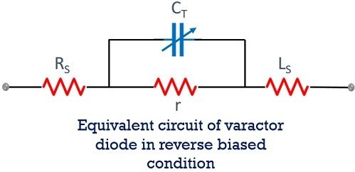
Here, RS represents series resistance, CT is transition capacitance, r denotes reverse diode resistance and LS is the series inductance or effective inductance. It is necessary to have the value of r to be very high. Hence, silicon is generally used in fabricating varactor diodes.
Characteristic Curve of Varactor Diode
The figure below represents the volt-amp characteristic of the varactor diode:
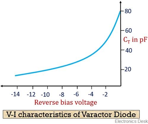
The graph shows the variation of junction capacitance with respect to the applied reverse voltage. As already discussed earlier that capacitance is inversely proportional to width so with the reverse voltage. Thus, we can see an exponential fall in the transition capacitance with the rise in voltage.
The relation between capacitance and the voltage provided is given by the equation:
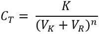
: K denotes the constant that depends on the semiconductor material and fabrication method
VK denotes the barrier potential
VR is the reverse applied potential
And n is a constant that depends on doping level. Usually, its value is 1/2 for alloyed junctions and 1/3 in case of diffused junctions.
The transition capacitance in case of no applied voltage is given as:
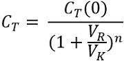
Low capacitance indicates that the charge stored is less. Therefore, if we want to have more charge storage the potential must be kept as low as possible.
Applications of Varactor Diode
As it exhibits voltage-controlled capacitance characteristic thus they have taken the place of mechanically tuned capacitors. Varactor diodes are widely used in TV sets and radios operating at high frequencies. These also finds its application in Bandpass filters, amplifiers and frequency multipliers.
Key terms related to Varactor Diode
- Transition capacitance: Its another name is depletion region capacitance or junction capacitance. Transition capacitance is defined as the variation in the capacitance with the applied voltage. It is denoted by CT. Its value is inversely proportional to the reverse voltage provided to it.
- Permittivity: Permittivity is the property that determines the charge stored by the dielectric material on applying a unit voltage to it.
- Dielectric: A dielectric or dielectric material shows bad electrical conductance. That means it does not allow electric current to flow through it. However, the charge storage of a dielectric medium is much better in comparison to a vacuum.
So, we can conclude that a varactor diode possesses variable capacitance characteristic with the applied reverse bias potential. It is inexpensive and a reliable device.
Nice 👍 explanation. Please add electrical contents also