Definition: JFET is the shortened form for Junction Field Effect Transistor. It is a 3 terminal semiconductor device in which current conduction takes place only due to the flow of majority charge carriers. Thus, it is a unipolar transistor.
The 3 terminals of the JFET are source, drain and gate. Unlike BJT, JFET is a voltage controlled device as here the potential applied at the gate terminal controls the drain current.
JFET is majorly categorized as n-channel and p-channel. These two are mainly classified on the basis of the basic semiconductor material used at the time of fabrication. Or we can say, the majority carriers that are responsible for the flow of current through the device.
As in an n channel JFET, the n-type silicon substrate is taken and 2 p-type semiconductor bars are diffused on it. Thereby generating a channel for the flow of electron. Thus known as n channel JFET.
While, in a p channel JFET, the p-type silicon substrate is taken and 2 n-type semiconductor materials are diffused on it. Hence, generating a channel for current conduction referred as p channel JFET.
Construction of JFET
As we have already discussed here that a JFET is classified as n channel and p channel according to the fabrication. So, in this section, we will discuss the constructional details of n channel JFET.
For constructing n-channel JFET, an n-type semiconductor substrate (usually silicon is used) is taken. Over the n-type bar, 2 small p-type silicon bars are diffused. But it is to be noted here that, these small bars are to be diffused on the two opposite sides of the substrate.
The figure below represents the constructional representation of an n channel JFET:
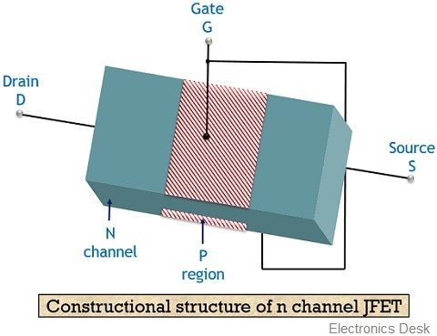
After the diffusion of the p-type material over the n-type material, the leftover region in n substrate is called as a channel through which majority charge carriers (i.e., electrons) flow. Once the channel is formed, then metallization of both the ends of the channel is performed in order to form the source and drain terminals.
Also, the two diffused silicon bars that form the pn junctions in the channel are connected together so as to form the gate terminal of the structure.
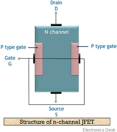
Let us now have a look at the structural representation of the JFET:
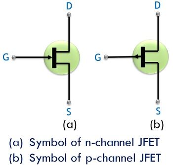
Symbol of JFET
Let us have a look at the symbolic representation of both n-channel and p-channel JFET:
Working of JFET
Let us now assume 3 cases in order to understand the operation of the n channel JFET:
Case 1: When no external potential is provided to neither gate nor drain corresponding to the source terminal. This means
VGS = VDS = 0
So, in this case, the two pn junctions will have depletion regions of the same thickness. As no any external biasing is provided, this means due to temperature variation the majority charge carriers (electrons) move from source to the drain terminal.
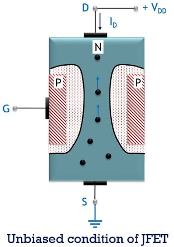
Due to this conduction takes place in the direction from drain to source i.e., opposite to the direction of flow of carriers. Hence, the current is termed as the drain current.
It is noteworthy here that in unbiased condition a thin depletion region exists between the two pn junctions which are shown clearly in the above figure.
Case 2: When a small voltage is provided between the gate-source terminal. This means
VGS ≠ 0
So, in this condition, when the small reverse potential is provided between gate to source terminal then the reverse voltage enhances (increases) the depletion width of the pn junctions.
Also, we know n channel exhibits resistive nature. So, the voltage drop is noticed in the channel. This is due to the current flowing between the terminals drain and source.
Due to the voltage drop, the two junctions becomes more reverse bias thereby causing the depletion region to penetrate more into the channel.
The figure below represents the non-uniform penetration of the 2 depletion regions into the channel:
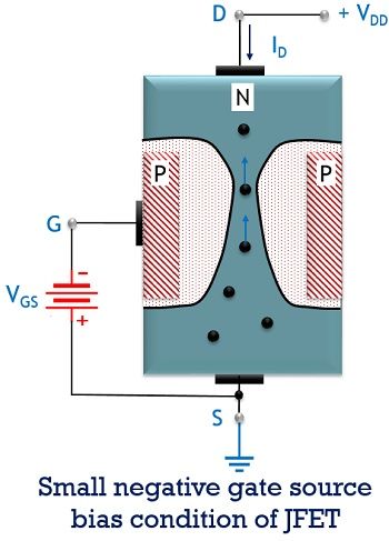
As the above figure clearly represents that the width of the depletion region is more towards the drain side than the source side. This is so because the voltage drop at the drain is comparatively higher than the voltage at the source side.
This clearly implies that the reverse biasing provided to the terminal is non-uniform over the channel i.e., it is more near the drain than the source.
Due to the increase in the depletion width, the channel region for the flow of electrons gets reduced. This results in a reduction in the current flowing from drain to source terminal.
Case 3: When high gate to source reverse potential is applied.
So, in this case, due to the high reverse gate-source voltage, the depletion width increases further. At the higher gate to source voltage, a point is reached where the two depletion layers meet each other.
The below figure clearly shows the joining of the depletion layer with high gate voltage:
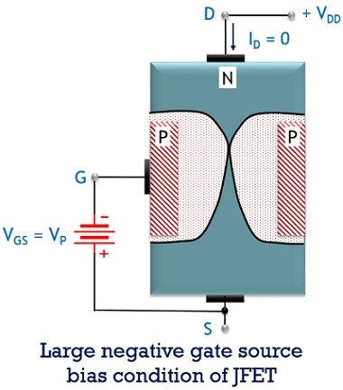
This will lead to completely blocking some region of the channel thereby blocking the movement of majority charge carriers.
Due to this, the flow of current through the channel totally cuts off. So, the particular gate to source voltage that totally stops the conduction through the device is known as cut-off or pinch-off voltage.
It is noteworthy here that with the decrease in the reverse applied voltage at the gate terminal the channel resistance also shows a reduction. Resultantly, causing a rise in the drain current.
Advantages of JFET
- A junction field effect transistor produces less noise during operation as only majority charge carriers are responsible for its conduction.
- A JFET consumes less power during the operation.
- As it a small size device hence occupies less space.
- It offers large input impedance.
Disadvantages of JFET
- The product of gain-bandwidth is small in case of JFET.
- Its cost is high.
- The small device size sometimes causes difficulty in handling.
Applications of JFET
- In op-amp: As it is a voltage controlled device. Thus, it finds applications as a voltage variable resistor in operational amplifiers.
- In RF amplifiers: The noise generating level of a JFET is very low as compared to other electronic devices. Thus these are widely used for radio frequency amplification.
- In switching circuits: As the current through the device depends on the gate applied a voltage in case of FETs. Thus these are used in switching applications.
- In digital circuits: The small structure of the device permits its use in digital circuits and memory units of computer systems.
Key terms related to JFET
- Source: It is the terminal that forms a connection with one end of the channel. Basically, the source terminal provides majority charge carriers whose movement generates a current through the device.
- Drain: Drain terminal is present at the opposite end of the source terminal. The majority charge carriers move from an end to other and get collected at the drain terminal of the transistor.
- Gate: This terminal is formed by a combined connection of the two heavily diffused regions over the substrate. The voltage that controls the level of current is provided at the gate terminal.
- Channel: It is the region present between gate and source terminal through which movement of majority carriers takes place.
- Pinch-off voltage: It is the maximum reverse voltage applied at the gate to the source terminal, that eventually causes the gate current to become zero.
So, from the above discussion, it is clear why the device is termed as junction field effect transistor. As here, the electric field generated by the reverse gate voltage is responsible for controlling the drain current.