Definition: Photovoltaic cells are basically those semiconductor devices that show sensitivity towards light. It has the ability to change radiation energy into equivalent electrical energy. The name of the device itself shows its operation. As the word photo is used for light and voltaic is used for electricity.
Photovoltaic cells are also known as solar cells as it makes use of solar energy in general basis. However, it is not necessary that we only use a natural source of light energy as one can also make use of an artificial light source at the time of operation of photovoltaic cells. It produces a proportional voltage as the output of incident radiation. The working principle of the device is based on the photovoltaic effect.
Now the question arises what is Photovoltaic Effect?
So, a photovoltaic effect is a combination of a physical and chemical process that generates a potential difference when the device is exposed to radiation. This generated voltage corresponds to the intensity of incident radiation.
It is to be noteworthy in the case of solar cells that it does not need an external voltage source. As due to the applied illumination a proportionate voltage is generated at the junction of the device.
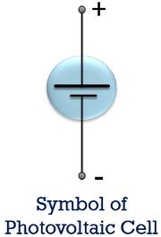
Symbol of Photovoltaic Cell
The symbolic representation of a photovoltaic cell is given below:
Construction of Photovoltaic cell
The photovoltaic cell is a semiconductor pn junction device. However, its construction is not the same as a normal junction diode.
It is formed by a combination of p-type semiconductor material with an n-type semiconductor. Usually, silicon and selenium are used as the basic semiconductor material. However, gallium arsenide, cadmium sulphide are also majorly used.
The figure below represents the cross-sectional arrangement of a solar cell:
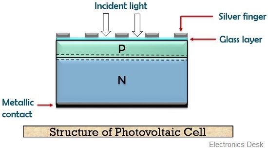
Here, the above figure clearly represents that the top layer of the device i.e., p region is made very thin in comparison to n region.
The reason why we have constructed the two regions differently is that the region from where the light ray is allowed to incident must be thin. So, that the incident radiation can easily penetrate to the depletion region (pn junction).
A layer of glass is placed at the top surface of the device in order to gather maximum incident radiation. Also, metallic fingers are provided at the top surface of the structure. Here, we have used silver fingers. As they are good conductors and absorbs the released electrons easily in order to provide proper conduction.
Now, the question arises why we have placed the silver fingers at some distance with the other?
The answer is that if we place a layer of metal at the top surface then it does not allow the penetration of radiation to the depletion region. So, it is placed in such a way that light rays can easily reach the junction region.
Also at the bottom, a metallic contact is placed which is generally a nickel plating that acts as negative contact for the whole structure.
Working of Photovoltaic cell
As we have already discussed at the beginning of the article that photovoltaic cells or solar cells are light sensitive devices that produce an electric voltage or current when its surface is illuminated with radiation.
So, now have a look at how potential difference is generated when no external potential is provided but a light ray is incident on it.
The figure below represents a detailed structure showing the working of the solar cells:
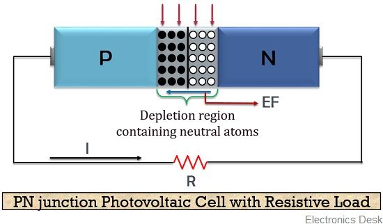
When no any light energy is provided to the device then the device does not conduct. Only the intensity of radiation falling at the surface allows a proportional current to flow through the device.
When a light ray is permitted to incident at the top surface of the structure. Then the glass placed gathers the light energy and permit it to reach the p region. As at the time of construction we have discussed that the thin p region is fabricated in order to have easy light penetration towards the junction region.
We know that junction is depletion region composed of neutral atoms. Thus, when a light ray incident at the junction then it produces electron-hole pairs. Due to the presence of depletion region an electric field exists.
Under the influence of the electric field, electrons move to the N side and holes drift towards the P side. In this way, the movement of charge carriers generates an electric current through the device.
However, it is to be noted here that the material is a semiconductor. Hence, it does not permit easy flow of charge carriers. So, to have a sufficient amount of current flow to take place metallic fingers are fabricated at the top surface.
These metallic fingers are nothing but conducting rods that easily absorbs the emitted electrons. This phenomenon gives rise to a potential difference. The generated emf is known as photovoltage. As the voltage is produced due to light.
It is to be noted here that the energy of the incident radiation (or photon energy) must be greater than the energy band gap between valence and conduction band. This is so because in order to have proper conduction electron must be free to get excited to the conduction band.
In this way, an electric potential is generated by a photovoltaic cell without using external bias. It generates voltage nearly from 0.5 to 0.6V.
If we want to increase the overall output through the device, then multiple photocells can be parallelly connected.
Output Characteristic of Photovoltaic cells
The figure below represents the output voltage characteristic of a solar cell:
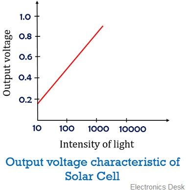
Here x-axis represents the intensity of incident light and the y-axis shows the output voltage produced. We can see here that with the increase in the intensity of the light there is an increase in the output voltage produced.
Moving further have a look at the output current characteristics of a solar cell with different load resistances:
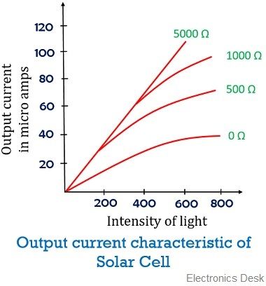
Here also with the increase in the intensity of light the resultant current through the cell also increases. The output current is low and its value lies in microamperes. The achieved output current relies on the intensity of incident radiation, the size of the cell structure and the conversion efficiency of the device.
Advantages of Photovoltaic Cell
- These devices have a long life span as they are highly durable.
- It only requires excitation through light energy.
Disadvantages of Photovoltaic Cell
- It is expensive.
- The presence of light source is necessary.
- As it generates low output thus for high scale production large solar cells are required.
Applications of Photovoltaic Cell
Solar cells are widely used in space satellites systems. These also find its applications in light meters and solar power charging devices as it efficiently utilizes solar energy.