Definition: 8086 is a 16-bit microprocessor and was designed in 1978 by Intel. Unlike, 8085, an 8086 microprocessor has 20-bit address bus. Thus, is able to access 220 i.e., 1 MB address in the memory.
As we know that a microprocessor performs arithmetic and logic operations. And an 8086 microprocessor is able to perform these operations with 16-bit data in one cycle. Hence is a 16-bit microprocessor. Thus the size of the data bus is 16-bit as it can carry 16-bit data at a time. The architecture of 8086 microprocessor, is very much different from that of 8085 microprocessor.
We have already discussed the introduction to the microprocessor and 8085 microprocessor. So, lets now proceed further and understand the architecture and working of 8086 microprocessor.
Block Diagram of 8086 Microprocessor
The architecture of 8086 microprocessor is composed of 2 major units, the BIU i.e., Bus Interface Unit and EU i.e., Execution Unit. The figure below shows the block diagram of the architectural representation of the 8086 microprocessor:
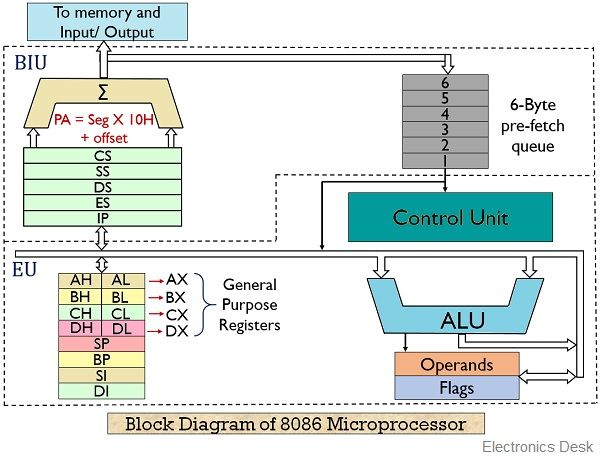
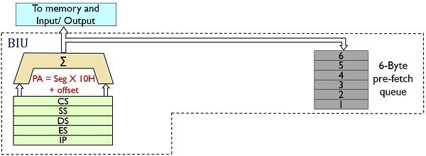
Bus Interface Unit (BIU)
The Bus Interface Unit (BIU) manages the data, address and control buses.
The BIU functions in such a way that it:
- Fetches the sequenced instruction from the memory,
- Finds the physical address of that location in the memory where the instruction is stored and
- Manages the 6-byte pre-fetch queue where the pipelined instructions are stored.
An 8086 microprocessor exhibits the property of pipelining the instructions in a queue while performing decoding and execution of the previous instruction. This saves the processor time of operation by a large amount. This pipelining is done in a 6-byte queue. Also, the BIU contains 4 segment registers. Each segment register is 16-bit. The segments are present in the memory and these registers hold the address of all the segments. These registers are as follows:
1.Code segment register: It is a 16-bit register and holds the address of the instruction or program stored in the code segment of the memory.
Also, the IP in the block diagram is the instruction pointer which is a default register that is used by the processor in order to get the desired instruction. The IP contains the offset address of the next byte that is to be taken from the code segment.
2. Stack segment register: The stack segment register provides the starting address of the stack segment in the memory. Like in stack pointer, PUSH and POP operations are used in this segment to give and take the data to/from it.
3. Data segment register: It holds the address of the data segment. The data segment stores the data in the memory whose address is present in this 16-bit register.
4. Extra segment register: Here the starting address of the extra segment is present. This register basically contains the address of the string data.
It is to be noteworthy that the physical address of the instruction is achieved by combining the segment address with that of the offset address.
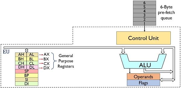
6-byte pre-fetch queue: This queue is used in 8086 in order to perform pipelining. As at the time of decoding and execution of the instruction in EU, the BIU fetches the sequential upcoming instructions and stores it in this queue.
The size of this queue is 6-byte. This means at maximum a 6-byte instruction can be stored in this queue. The queue exhibits FIFO behavior., first in first out.
Execution Unit (EU)
The Execution Unit (EU) performs the decoding and execution of the instructions that are being fetched from the desired memory location.
Control Unit:
Like the timing and control unit in 8085 microprocessor, the control unit in 8086 microprocessor produces control signal after decoding the opcode to inform the general purpose register to release the value stored in it. And it also signals the ALU to perform the desired operation.
ALU:
The arithmetic and logic unit carries out the logical tasks according to the signal generated by the CU. The result of the operation is stored in the desired register.
Flag:
Like in 8085, here also the flag register holds the status of the result generated by the ALU. It has several flags that show the different conditions of the result.
Operand:
It is a temporary register and is used by the processor to hold the temporary values at the time of operation.
The reason behind two separate sections for BIU and EU in the architecture of 8086 is to perform fetching and decoding-executing simultaneously.
Working of 8086 Microprocessor
In the previous section, we have discussed the operation of various sections of the BIU and EU. Now in this section, we will have a look at the overall processing cycle of the 8086 microprocessors. So, basically, when an instruction is to be fetched from the memory, then firstly its physical address must be calculated and this is done at the BIU. The physical address of an instruction is given as:
PA = Segment address Χ 10 + Offset
For example: Suppose the segment address is 2000 H and the offset address is 4356 H. So, the generated physical address is 24356 H. Here, the code segment register provides the base address of the code segment which is combined with the offset address.
The code segment contains the instructions. Each time an instruction is fetched the offset address inside the code segment gets incremented. So, once the physical address of an instruction is calculated by the BIU of the processor, it sends the memory location by the address bus to the memory. Further, the desired instruction at that memory location which is present in the form of the opcode is fetched by the microprocessor through the data bus.
Suppose the instruction is ADD BL, CL. But, inside the memory, it will be in the form of an opcode. So, this opcode is sent to the control unit.
The control unit decodes the opcode and generates control signals that inform the BL and CL register to release the value stored in it. Also, it signals the ALU to perform the ADD operation on that particular data.
It is noteworthy that in any instruction, like ADD BL, CL. BL denotes the destination of the result of the add operation. This clearly shows that whatever, the operation is performed its result must be stored in the first register i.e., BL for this particular example.
Let us take another example: Consider an instruction, ADD CL, 05H.
This means that the operand which is 05H is to be added with the data present in the CL register and is stored in that particular register i.e., CL. In such conditions, the operand is not provided to the control unit as only the opcode is required to be decoded by the CU. Hence the operand is directly provided to the ALU. Also, the status of this result is stored in the flag register. So, whenever, ALU carries out an operation, it simultaneously generates the result as well as its status.
It is to be noteworthy that in BIU, pipelining fails whenever there is branching in the instruction. This is because generally instructions are present in a sequential manner. But, sometimes the instructions are required to be executed unsequentially. However, in the queue, the instructions are stored sequentially. So, in case there exist a need for any random instruction to be decoded. The opcode stored in the queue will become invalid and must be cleared at that particular time.
So, this is all about the block diagram and working of 8086 microprocessor.
Thanks…!
great article
Great and helpfull🙏❤️