8255 is a programmable I/O device that acts as interface between peripheral devices and the microprocessor for parallel data transfer. 8255 PPI (programmable peripheral interface) is programmed in a way so as to have transfer of data in different conditions according to the need of the system.
In 8255, 24 pins are assigned to the I/O ports. Basically it has three, 8-bit ports that are used for simple or interrupt I/O operations.
The three ports are Port A, Port B and Port C and as each port has 8 lines, but the 8 bits of port C is divided into 2 groups of 4-bit each. These are given as port C lower i.e., PC3 – PC0 and port C upper i.e., PC7 – PC4. And are arranged in group of 12 pins each thus designated as Group A and Group B.
The two modes in which 8255 can be programmed are as follows:
- Bit set/reset mode
- I/O mode
The bits of port C gets set or reset in the BSR mode. The other mode of 8255 i.e., I/O mode is further classified into:
Mode 0: Simple input/output
Mode 1: Input output with handshaking
Mode 2: Bidirectional I/O handshaking
Mode 1 and Mode 2 both are same but the only difference is mode 1 does not support bidirectional handshaking.
This means if 8255 is programmed to mode 1 input, then it will particularly be connected to an input device and performs the input handshaking with the processor.
But if it is programmed to mode 2 then due to bidirectional nature, the PPI will perform both input and output operation with the processor according to the command received.
Architecture of 8255 PPI
The figure below represents the architectural representation of 8255 PPI: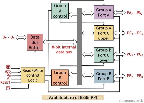
Let us understand the operation performed by each unit separately.
Data bus buffer: It is used to connect the internal bus of 8255 with the system bus so as to establish proper interfacing between the two. The data bus buffer allows the read/write operation to be performed from/to the CPU.
The buffer allows the passing of data from ports or control register to CPU in case of write operation and from CPU to ports or status register in case of read operation.
Read/ Write control logic: This unit manages the internal operations of the system. This unit holds the ability to control the transfer of data and control or status words both internally and externally.
Whenever there exists a need for data fetch then it accepts the address provided by the processor through the bus and immediately generates command to the 2 control groups for the particular operation.
Group A and Group B control: These two groups are handled by the CPU and functions according to the command generated by the CPU. The CPU sends control words to the group A and group B control and they in turn sends the appropriate command to their respective port.
As we have discussed that group A has the access of the port A and higher order bits of port C. While group B controls port B with the lower order bits of port C.
CS: It stands for chip select. A low signal at this pin shows the enabling of communication between the 8255 and the processor. More specifically we can say that the data transfer operation gets enabled by an active low signal at this pin.
RD – It is the signal used for read operation. A low signal at this pin shows that CPU is performing read operation at the ports or status word. Or we can say that 8255 is providing data or information to the CPU through data buffer.
WR – It shows write operation. A low signal at this pin allows the CPU to perform write operation over the ports or control register of 8255 using the data bus buffer.
A0 and A1: These are basically used to select the desired port among all the ports of the 8255 and it do so by forming conjunction with RD and WR. It forms connection with the LSB of the address bus.
The table below shows the operation of the control signals:
| A1 | A0 | RD' | WR' | CS' | Input/Output Operation |
|---|---|---|---|---|---|
| 0 | 0 | 0 | 1 | 0 | Port A - Data Bus |
| 0 | 1 | 0 | 1 | 0 | Port B - Data Bus |
| 1 | 0 | 0 | 1 | 0 | Port C - Data Bus |
| 0 | 0 | 1 | 0 | 0 | Data Bus - Port A |
| 0 | 1 | 1 | 0 | 0 | Data Bus - Port B |
| 1 | 0 | 1 | 0 | 0 | Data Bus - Port C |
| 1 | 1 | 1 | 0 | 0 | Data Bus - Control register |
Reset: It is an active high signal that shows the resetting of the PPI. A high signal at this pin clears the control registers and the ports are set in the input mode.
Initializing the ports to input mode is done to prevent circuit breakdown. As in case of reset condition, if the ports are initialized to output mode then there exist chances of destruction of 8255 along with the processor.
Pin Diagram of 8255 PPI
The figure below represents the 40 pin configuration of 8255 programmable peripheral interface:
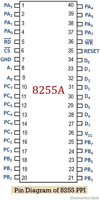 As we can see that pin number 27 to 34 is allotted to data bus. These are tri-state data bus lines of bidirectional nature that connects 8255 with the processor. These are used to allows flow of data and control or status word between the 8255 and the processor.
The external voltage required to drive the circuit is provided at pin number 26 i.e., VCC. Also pin number 7 is the ground connection of the circuit.
Out of 40 pins, 24 pins are allotted to I/O ports. Rest of the pins are allotted to the signals discussed above.
Modes of Operation
As we have already discussed that 8255 has two modes of operation. These are as follows:
Bit Set-Reset mode: When port C is utilized for control or status operation, then by sending an OUT instruction, each individual bit of port C can be set or reset.
I/O mode: As we know that the I/ O mode is sub-classified into 3 modes. So, let us now discuss the 3 modes here.
Mode 0: Input/Output mode
This mode is the simple input output mode of 8255 which allows the programming of each port as either input or output port. The input/output feature of mode 0 includes:
- It does not support handshaking or interrupt capability.
- The input ports are buffered while outputs are latched.
Mode 1: Input/Output with handshaking
Mode 1 of 8255 supports handshaking with the ports programmed as either input or output mode. We know that it is not necessary that all the time the data is transferred between two devices operating at same speed. So, handshaking signals are used to synchronize the data transfer between two devices that operates at different speeds.
The figure below shows the data transferring between CPU and an output device having different operating speeds:
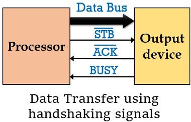
- Here STB signal is used to inform the output device that data is available on the data bus by the processor.
- Here port A and port B can be separately configured as either input or output port.
- Both the port utilizes 3-3 lines of port C for handshaking signals. The rest two lines operates as input/output port.
- It supports interrupt logic.
- The data at the input or output ports are latched.
Mode 2: Bidirectional I/O port with handshaking
In this mode, the ports can be utilized for the bidirectional flow of information by handshaking signals. The pins of group A can be programmed to acts as bidirectional data bus and the port C upper (PC7 – PC4) are used by the handshaking signal. The rest 4 lower port C bits are utilized for I/O operations.
As the data bus exhibits bidirectional nature thus when the peripheral device request for a data input only then the processor load the data in the data bus. Port B can be programmed in mode 0 and 1. And in mode 1 the lower bits of port C of group B are used for handshaking signals.
So, from the above discussion it is clear that how interfacing of peripheral devices is performed with the processor.