Definition: 8085 is an 8-bit microprocessor as it operates on 8 bits. The size of the address bus in 8085 is 16 bits. Thus, can address 64 KB memory. An 8085 microprocessor is an IC with 40 pins and operates with +5V power supply.
The pin configuration plays a very important role in understanding the architecture of 8085 microprocessor. So, now let’s move further and understand how the processor operates inside any system with these 40 pins.
But before that have a look at the pin diagram of 8085 microprocessor.
Pin Diagram of 8085 Microprocessor
The figure below shows the pin diagram of 8085 showing 40 pin configuration:
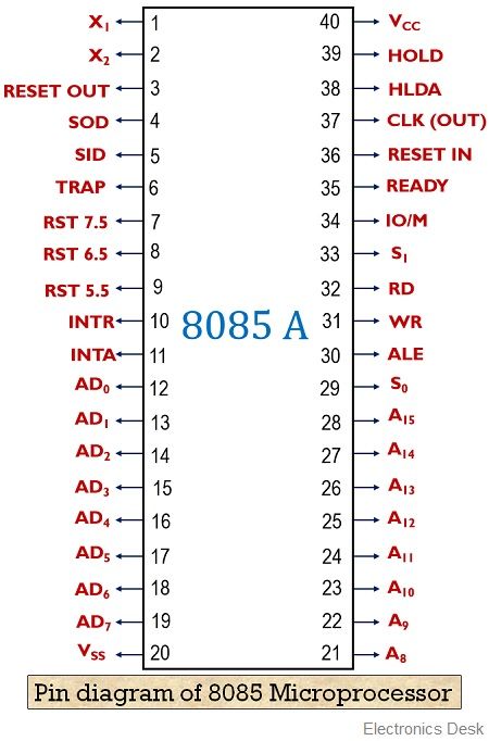
The signals of this 40 pin IC is grouped into 7 categories, which are given below:
- Power supply and clock signals
- Data bus
- Address bus
- Serial I/O ports
- Control and status signals
- Interrupts and externally generated signals
- Direct memory access
These are the categories among which the 40 pin configuration of 8085 is divided. So, let us proceed to understand the role of each pin inside the 8085 microprocessor.
Pin Description of 8085 Microprocessor
1.Power supply and clock signals:
In 40 pin configuration, 4 pins are allotted to this particular category.
- VCC – Pin number 40 denotes VCC, and an external power supply of + 5 V is provided at this pin.
- VSS – Its pin number is 20. This pin shows the grounded connection of the microprocessor.
- X1 and X2 – These are represented by pin number 1 and 2 respectively in the pin configuration. These 2 pins are connected with a crystal or LC network to maintain the internal frequency of the clock generator.
- CLK (OUT) – It is the 37th pin of the 8085 IC and acts as the system clock that keeps the record of time duration required by each operation to get completed.
2.Address Bus – This category contains 8 pins.
The address bus has 16 lines i.e.; it can carry 16 bits at a time. However, out of 16, 8 are multiplexed with the data bus and the leftover 8 are separately shown by pin number 21 to 28 in the pin configuration.
These are used to carry the address of data and instruction from the processor to the memory location and is unidirectional in nature. These are denoted by A8 to A15 that represents the 8 MSB of the memory location or input-output address.
3.Data Bus with multiplexed address bus – This category also contains 8 pins.
The size of the data bus of the 8085 microprocessor is 8 bits. However, to reduce the number of bus lines these 8-bit data bus lines are multiplexed with the 8-bit address bus.
These are shown by pin number 12 to 19. The address bus is denoted by A whereas the data bus is denoted by D. The pin configuration denotes the lower order multiplexed address and data bus bits from AD0 to AD7.
We have already discussed that the address bus contains the address of the desired memory location from where the data or instruction is to be fetched. While the data bus contains the data or instruction that is needed to be fetched from the memory.
4.Serial I/O ports :
It has basically 2 pins.
- SID – SID denotes serial input data pin and its pin is numbered as 5. With this pin, data is serially fed to the processor directly through the input devices.
- SOD – SOD denotes serial output data pin and its pin number is 4, in the pin configuration of 8085. Once the data is processed in the microprocessor then this pin represents bit by bit results at the output devices.
5.Control and status signals :
Basically, 6 pins of the pin configuration are used by control and status signals.
- ALE – ALE is an acronym for address latch enable and is pin number 30 in the configuration. We know that 8 lower order bits of the 16-bit address bus are multiplexed with the 8-bit data bus.
This pin gets enabled at the time when the address is present at the multiplexed address and data bus. Otherwise, it gets disabled showing the absence of an address on the bus.
- RD – This pin is numbered 32 in the configuration and a low signal in this pin shows the read operation either from I/O devices or from the memory unit. Thereby indicating that the data bus is now in a state or position to accept the data from the memory or I/O devices.
- WR – It is the 31st pin in the pin diagram and a low signal in this pin represents the write operation at the memory or I/O devices. This indicates that the data present in the data bus is to be written into the desired memory address or I/O device by the processor.
- IO/M – It is pin number 34 and indicates the selection of a memory address or input-output device. This shows whether the read/write operation is to be carried out at the memory location or at the I/O device.
The low signal at this pin shows that operation is performing over memory location. As against, a high signal at this pin represents the operation at I/O device.
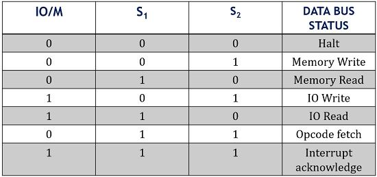
- S0 and S1 – The pins S0 and S1 represent the status signal at pin number 29 and 33 respectively. These signals show the type of recent operation of the microprocessor. The table below represents the status of the data bus under different conditions:
6.Interrupts and Externally generated signals:
Interrupts are the signals that are generated to break the sequence of an ongoing operation. When an interrupt signal is generated then CPU immediately stops its recent task under operation and switches to some other program known as interrupt service routine (ISR).
However, after handling ISR, the CPU gets back to its main program for execution.
In the pin configuration, 5 types of interrupts are shown by 5 different pins from pin number 6 to 10. These pins are used to manage the interrupt.
Basically, there exist 2 types of interrupts:
Maskable Interrupt and Non- maskable interrupt
Out of the 5 major interrupts 4 are the maskable interrupts. These are INTR, RST5.5, RST6.5, RST7.5 and are easily manageable interrupts.
However, TRAP is a non-maskable interrupt and holds the topmost priority among all interrupts in the 8085 microprocessor.
- RESET IN – It is pin number 36 in the pin diagram. An active low signal at this pin resets the PC of the microprocessor to 0. Or we can say, after resetting the PC holds its initial memory address.
- RESET OUT – It is the 3rd pin in the pin diagram. This pin generates a signal to provide information about the resetting of the microprocessor. Also, we can say that once a processor is reset then all the connected devices must also be reset.
So, enabling this signal shows the resetting of the interconnected devices.
- INTA: It is the 11th pin of the 8085 pin configuration. A signal at this pin acknowledges the generated interrupt.
7.Direct Memory Access (DMA) :
We are aware of the fact that memory and I/O devices are connected with each other by the microprocessor. So, the intermediator i.e., CPU manages the data transfer between the input-output device and memory.
However, when data in a large amount is to be transferred between I/O devices and memory the CPU gets disabled by tri-stating its buses. And this transfer is manageable by external control circuits. The DMA has 2 pins.
- HOLD – This signal is generated at pin number 39. This pin generates a signal to notify the processor that more than one request is present to access the data and address bus.
When this signal gets enabled, the CPU frees the bus after completion of the recent operation. Once the hold signal gets disabled, the processor can access the bus again.
- HLDA -This signal is generated at pin number 38. This signal is enabled at the time when the processor gets HOLD signal and it releases HLDA i.e., hold acknowledge signal. In order to show that the multiple requests are kept on hold and will be considered once the bus gets free after the recent operation.
After the disabling of hold request, the HLDA signal becomes low.
- READY -This is the 35th numbered pin in the pin diagram that maintains synchronization between the processor and peripherals, memory. It is clear that a microprocessor has a much faster response than peripherals and memory.
So, this pin is enabled when the processor as well as the peripherals and memory both become ready to begin the next operation.
In the case when the READY pin is disabled, then the microprocessor is in the WAIT state.
This is all about the pin description of the 8085 microprocessor.
Nice post
Very nice work ❤️. I really really like your work, it’s language is so easy to understand. Information like on this site is no where available on internet. It helps me a lot. Thank you very much.
Thanks a lot. Keep reading.
Very nice