80286 Microprocessor is a 16-bit microprocessor that has the ability to execute 16-bit instruction at a time. It has non-multiplexed data and address bus. The size of data bus is 16-bit whereas the size of address bus is 24-bit.
It was invented in February 1982 by Intel. 80286 microprocessor was basically an advancement of 8086 microprocessor. Further in 1985, Intel produced upgraded version of 80286 which was a 32-bit microprocessor.
Now the question arises what are the factors that make 80286 more advantageous than 8086 microprocessor?
- It has non-multiplexed address and data bus that reduces operational speed.
- The addressable memory in case of 80286 is 16 MB.
- It offers an additional adder for address calculation.
- 80286 has faster multipliers that lead to quick operation.
- The performance per clock cycle of 80286 is almost twice when compared with 8086 or 8088.
Operating modes of 80286 microprocessor
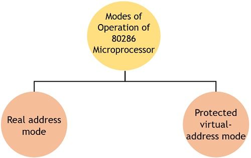
80286 operates in two modes:
In real address mode, this microprocessor acts as a version of 8086 which is quite faster. Also without any special modification, the instruction programmed for 8086 can be executed in 80286. It offers memory addressability of 1 MB of physical memory.
The protected virtual-address mode of 80286 supports multitasking because multiple programs can be executed using virtual memory. This mode of 80286 offers memory addressability of 16 MB of physical memory along with 1 GB of virtual memory.
As using virtual memory, space for other programs can be saved. Sometimes bulky programs also do exist that cannot be stored in physical memory, so virtual memory is utilized in order to execute large programs.
This mode is used in 80286, so that in case of memory failure in real address mode, it can stay in protected manner.
What is virtual memory?
Virtual memory is that part of hard disk which can be utilized for storing large instructions inside the system. This extra memory can be addressed by the computer other than the physical memory.
When there exists an instruction that is to be loaded in the memory but whose size is greater than the provided physical memory. Then some part of hard disk is used in order to store that instruction, which is known as virtual memory.
Architecture of 80286 Microprocessor
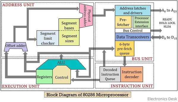
The figure below shows the architectural representation of 80286 microprocessor:
 As we have already mentioned earlier that it is a 16-bit microprocessor thus holds a 16-bit data bus and 24-bit address bus. Also, unlike the 8086 microprocessor, it offers non-multiplexed address and data bus, which increases the operating speed of the system.
80286 is composed of nearly around 125K transistors and the pin configuration has a total of 68 pins.
The CPU, central processing unit of 80286 microprocessor, consists of 4 functional block:
- Address Unit
- Bus Unit
- Instruction Unit
- Execution Unit
Firstly, the physical address from where the data or instruction is to be fetched is calculated, by the address unit. Once the physical address is calculated then the calculated address is handed over to the bus unit. More specifically we can say, that the calculated address is loaded on the address bus of the bus unit.
This address specifies the memory location from where the data or instruction is to be fetched. The fetching of data through the memory is done through the data bus. For faster execution of instruction, the BU fetches the instructions in advanced from the memory and stores them in the queue.
This is done through the bus control module. As we have discussed that the prefetched instructions are stored in a 6-byte instruction queue. This instruction queue then further sends the instruction to the instruction unit.
The instruction unit on receiving the instructions now starts decoding the instruction. As instructions are stored in prefetched queue thus the decoder continuously decodes the fetched instructions and stores them into decoded instruction queue.
Now after the instructions gets decoded then further these are needed to be executed. So, the instructions from decoded instruction queue are fed to the execution unit. The main component of EU is ALU i.e., arithmetic and logic unit that performs the arithmetic and logic operations over the operand according to the decoded instruction.
Once the execution of the instruction is performed then the result of the operation i.e., the desired data is send to the register bank through the data bus.
As we have already discussed that 80286 is just a modified version of 8086. The register set in 80286 is same as that of 8086 microprocessor.
- It holds 8 general purpose registers of 16 bit each.
- It contains 4 segment register each of 16-bit.
- Also has status and control register and instruction pointer.
Interrupt of 80286 Microprocessor
We know that whenever an interrupt gets generated in a system, then the execution of the current program is stopped and the execution gets transferred to the new program location where the interrupt is generated.
But once the interrupt gets executed then then in order to get back to the original program, its address as well as machine state must be stored in the stack. Basically there exist 3 categories of interrupt in 80286 microprocessor:
- External interrupt (Hardware interrupt)
- INT instruction interrupt (Software interrupt)
- Internally generated interrupt due to some exceptions
External or hardware initiate interrupt are those interrupts that gets generated due to an external input. And are basically of two types:
- Maskable interrupt
- Non-maskable interrupt
Sometimes when multiple programs are allowed to be executed in a system, then this leads to generation of INT instruction, and such an interrupt is known as software interrupt.
Another interrupt in 80286 exist due to some unusual conditions or situations generated in the system that leads to prevention of further execution of the current instruction.
So, this is all about the modes of operation, architecture and interrupts of 80286 microprocessor.
It was helpful for my Assignment.