Definition: 8086 is a 16-bit microprocessor and was created by Intel in 1978. Like the pin configuration of 8085 microprocessor, the 8086 microprocessor also contains 40 pins dual in line.
However, unlike the 8085 microprocessor, an 8086 to have better performance, operates in 2 modes that are minimum and maximum mode.
The minimum mode is a single processor configuration while the maximum mode is a multiple processor configuration.
Due to this reason, in the 40 pin IC of 8086 microprocessor, 8 pins i.e., pin numbered from 24 to 32 are assigned different configurations separately according to the two modes.
We will discuss the pin description in this section. But before that have a look at the pin diagram of 8086 microprocessor.
Pin Diagram 8086 Microprocessor
An 8086 microprocessor is also a 40 pin IC but has few separate pin configuration for minimum and maximum mode which we will discuss in this article.
The figure below represents the pin diagram of 8086 microprocessor:
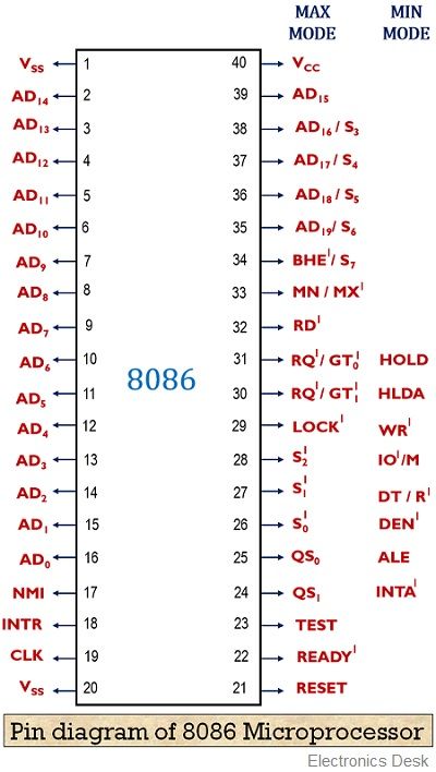
Here, from the above figure it is clear that from pin number 24 to 32, we have shown the different configuration for minimum and maximum mode. However, excluding these 8 pins, the rest 32 pins are the same for both minimum as well as maximum mode.
So, let us move further to understand the operation of each pin in the pin configuration of 8086.
Pin description of 8086 Microprocessor
VCC – Pin number 40 – At this pin, the external power supply of + 5V is provided to the processor.
VSS – Pin number 1 and 20 – These two pins acts as the ground. This pin directs the extra current of the microprocessor to ground.
AD0 – AD15 – Pin number 2 to 16 and 39 – These are the multiplexed address and data bus.
We know that the 8086 microprocessor has 20-bit address bus and 16-bit data bus. So, the 16 lines of the address and data bus are multiplexed together so as to reduce the number of lines inside the IC.
We are aware of the fact that at a time either address or data will be transmitted by the bus. So, at a particular time only either the address or the data bus will be enabled from the multiplexed buses.
A16/S3, A17/S4, A18/S5 and A19S6 – Pin number 35 to 38 – Out of 20 address bits, 4 are present in the multiplexed form with the status signals. In the case of memory operations, these pins act as an address bus and contain the memory address of any particular instruction or data.
However, from I/O operations these pins are low that shows the status of the processor.
Basically, the signal at S3 and S4 show that which segment is currently accessed by the microprocessor among the four segments present in it.
The table below will show the encoding of S3 and S4:
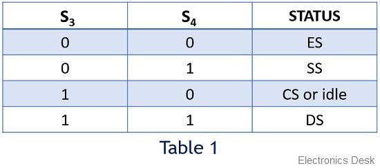
Also, S5, when enabled, shows the presence of an interrupts in the microprocessor. So, basically, it serves as an interrupt flag.
The signal at S6 shows the status of the bus master for the current operation. More simply we can say, whether the 8086 is the bus master or any other proficient device is acting as the bus master.
When 0 is present as the signal at this pin then it indicates the 8086 is holding the access of the bus otherwise it is high i.e., 1.
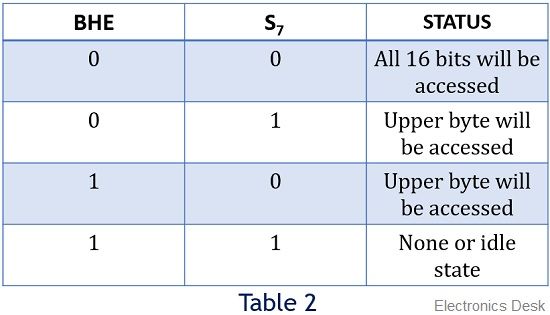
BHE’ / S7 – Pin number 34 – BHE is an acronym for Bus High Enable. The combination of the BHE signal and S7 status informs about the existence of the data on the bus. Also, different combinations show whether the bus is containing overall 16 bit, upper byte or lower byte of the data.
The table below represents the status for the signal at this pin:
MN/MX’ – Pin number 33 –The status at this particular pin shows whether the processor is operating in the minimum mode or maximum mode.
A signal 0 at this pin informs that the 8086 is operating in maximum mode i.e., multiple processors. While signal 1 shows the operation under minimum mode i.e., single processor.
RD’ – Pin number 32 – An active low signal at this pin shows that the microprocessor is performing read operation with either memory or I/O devices.
CLK – Pin number 19 – A signal at this pin provides the timing to the internal operations that are being executed inside the microprocessor.
NMI – Pin number 17 – NMI is Non-maskable interrupt. These are basically uncontrollable interrupts generated inside the processor. When an NMI occurs, then an interrupt service routine is generated by the interrupt vector table.
TEST – Pin number 23 – This pin basically shows the wait instruction. Whenever a low signal at this pin occurs then the processing inside the processor continues. As against, in case of the high signal, the processor has to wait for the disabling of this pin.
INTR – Pin number 18 – INTR stands for an interrupt request. The processor after each clock cycle samples the INTR and if the signal at this pin is found to be high then the processor controls that interrupt internally.
READY – Pin number 22 – This signal is used by the peripherals and memory devices in order to show the readiness for the next operation.
RESET – Pin number 21 – Whenever this pin is enabled then it resets the processor and other devices connected to the system by immediately terminating the recent task.
Pins in Minimum mode
INTA’ – Pin number 24 – It is an interrupt acknowledge pin. Whenever an INTR signal is generated, then the microprocessor generates INTA signal, as a response to that interrupt.
ALE – Pin number 25 – ALE is an abbreviation for address latch enable. Whenever an address is present in the multiplexed address and data bus, then the microprocessor enables this pin.
This is done to inform the peripherals and memory devices about fetching of the data or instruction at that memory location.
DEN’ – Pin number 26 – DEN is used for data enable. This is an active low pin that means whenever a 0 is present at this pin then the transceiver gets enabled and it separates the data from the multiplexed address and data bus.
DT/R’ – Pin number 27 – This pin is used to show whether the data is getting transmitted or is received. A high signal at this pin provides the information regarding the transmission of data. While a low indicates reception of data.
M/IO’ – Pin number 28 – This pin indicates whether the processor is performing an operation with memory or I/O devices. Whenever a high is present at this pin then it shows the operation is carried out through the memory. While a low signal shows operation through I/O devices.
WR’ – Pin number 29 – An active low signal at this pin indicates that the processor is performing write operation from either memory or I/O devices.
HOLD – Pin number 31 – When an external device enables this pin then the processor stops accessing the buses immediately after the recent task gets over.
HLDA – Pin number 30 – This pin is used as a response pin for the hold request. Once request for accessing the buses is produced by an external entity. Then the microprocessor acknowledges the device that its request will be considered once it gets over by the current operation.
Pins in Maximum mode
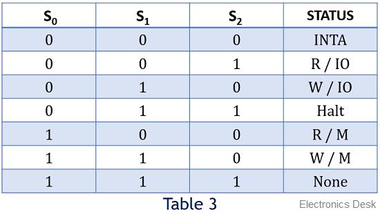
S0‘, S1‘ and S2‘ – Pin number 26 to 28 – These are basically 3 status pins and are active low. This means that if the status at all the 3 pins is 0 then it shows that multiple interrupts are to be handled in maximum mode.
The table below is representing the status of the processor in different combinations:
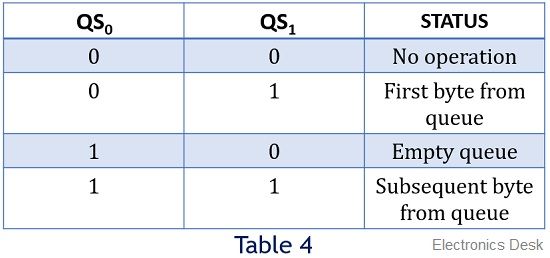
QS0 and QS1 – Pin number 24 and 25 – These two pins indicate the status of the 6-byte pre-fetch queue present in the architecture of 8086.
LOCK’ – Pin number 29 –This pin is involved in maximum mode operation. So, basically, when a single processor is accessing the buses and peripherals then it locks the resources being used by it. So, that no other entity can access it until the recent processor frees it.
RQ’/ GT0‘ and RQ’/ GT1‘ – Pin number 30 and 31 – Due to the involvement of multiple processors, these pins indicate the request and grant permission for accessing the buses, memory and peripherals.
This is all about the pin diagram and description of the 8086 microprocessor.