Definition: A circuit that is capable of sampling the input signal applied to its terminal as well as holding the sampled value up to the last sample for a particular time interval is known as sample and hold circuit. It basically utilizes an analog switch and a capacitor to perform the task.
The circuit samples the input signal in the time interval between 1 to 10 microsecond. Along with that holds the sampled value until another sampling command is provided to it.
The figure below represents the basic circuit for the sample and hold circuit:
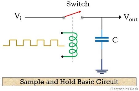
In the sample mode of the circuit, the switch present is closed, and so this charges capacitor C, with the instantaneous value of the applied input signal. However, in the hold mode of the circuit, the switch now gets open, and so no further charging is possible.
But now at the hold mode, the capacitor holds the charge that was initially being stored at the time of sample mode.
While the question arises that why the stored charge is held by capacitor rather being dissipated. So, this is because the circuit has no path for the dissipation of the stored charge through it.
Content: Sample and Hold Circuit
Need for Sample and Hold Circuit
We already know that digital communication is advantageous when compared with analog communication. However, to utilize a digital system, the applied signal at the input must also be in digitized form.
While originally, a signal is analog in nature. So, in order to change the analog signal into digital form, a sample and hold circuit is used. It is usually placed before an analog to digital converter.
Basically the sample and hold circuit, samples the analog signal and the capacitor present holds these samples. This sampled value when provided to the ADC, it generates a discrete signal from an analog one.
Let’s first see the input and output response of a sample and hold circuit:
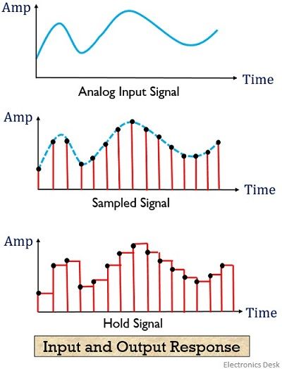
The first diagram in the above figure represents an analog signal that is applied at the input of the sample and hold circuit.
The sampling of the applied input signal in the closed switch condition is shown in the next image. While hold input of the analog signal under open switch condition is represented in the last image of the above figure.
Circuit Diagram
The figure below represents the practical sample and hold circuit:
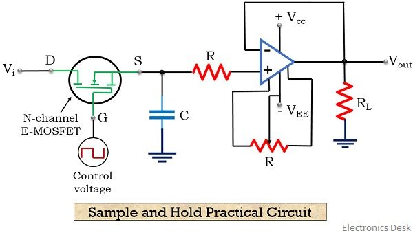
As we can see in the figure above that the circuit is composed of an E-MOSFET along with a capacitor and an op-amp. The enhancement type MOSFET acts as switch, whose conducting and the non-conducting state decides the sampling and holding duration of the circuit.
Working of Sample and Hold Circuit
As we can see in the practical representation of the circuit, that input voltage Vi is applied at the drain terminal of E-MOSFET. Also, a sample and hold control voltage, Vs is provided at the gate terminal of the E-MOS.
It is noteworthy here that the applied input signal is analog in nature while the control voltage applied at the gate terminal is a square wave. So, at the time when input is provided at the drain terminal and positive pulse of control signal Vs is applied at the gate terminal, then due to this, the MOSFET comes in conducting state.
Due to the conducting state, the MOSFET acts as a closed switch. And this leads to the charging of the capacitor present in the circuit with the input applied voltage.
This charging duration of the capacitor is said to be the sampling interval, and at this time, the overall input appears at the output as well as at the capacitor.
As we can see in the circuit shown above that the signal at the source of the MOSFET is fed to the non-inverting terminal of the op-amp through a resistor R. Also the output of the op-amp is provided at the inverting terminal of the op-amp.
So, the output of the op-amp will be same as that of input. Thus it is a non-inverting voltage follower circuit. This voltage follower circuit offers very high input impedance to the charge stored at the capacitor. Thus the stored charge at the capacitor is unable to get dissipated.
Further, when the voltage applied at the gate terminal of the transistor is 0, then the E-MOS comes in a non-conducting state. Due to this, it acts as an open switch, and input, in this case, will not appear at the source.
But at this particular condition, though the capacitor is not getting charged or discharged, it is holding the voltage by which it was charged at the sampling interval.
Thus we can say the duration at which charging of the capacitor takes place is known as the sample period. While the duration for which the voltage across the capacitor remains constant is the hold period of the circuit.
At the sampling period, the output will be equal to the input, however, at the hold period, the output will be equal to the previously sampled value.
It is to be kept in mind that the frequency of control signal, must be necessarily more than that of the applied input signal.
The figure below represents the typical connection diagram of the sample and hold circuit, where a sample and hold IC LF398 is used:
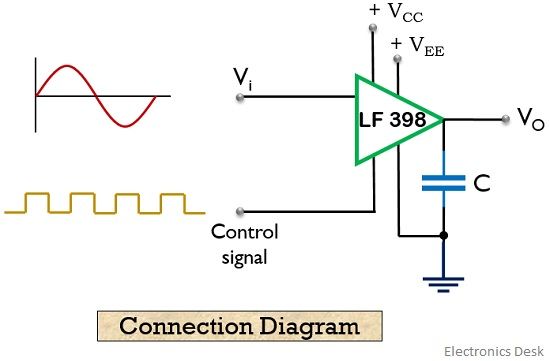
As we can see that one pin of the IC is provided with analog input while at the other pin, the control voltage is fed. Further, the sample and hold signal is generated.
Input and Output Waveforms
Let us now have a look at the waveform representation of input and output waveform of the signal at the sample and hold circuit.
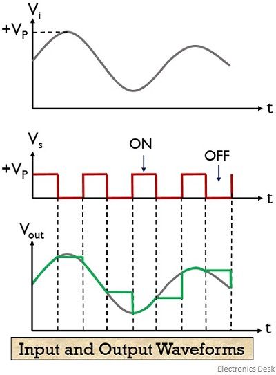
As we can see that the input to the sample and hold circuit is a continuous signal, while the output is a discrete signal. This is so because, despite the continuous change in the input signal, the output on being sampled holds that particular value and does not vary with the change in the input signal value.
In this way, a sample and hold circuit samples the applied signal and holds a particular value until the desired time period.
Advantages
- It provides synchronization to all the channel present in multi-channel analog to digital converter.
- The possibility of cross-talk can also be reduced.
Applications of Sample and Hold Circuit
- It is used in analog signal processing.
- Also finds applications in digital voltmeter.
- In the data conversion system as well as in sampling oscilloscopes.
- In data distribution systems and analog to digital converters.
- In filters used for signal construction.
This is all about the sample and hold circuit, introduction, circuit representation and working with applications.