8284 clock generator is an IC developed by Intel to provide clock frequency, ready and reset signal to the 8086/8088 microprocessor. It is an 18 pin chip.
8284 produces the clock signal, synchronizes it with the ready and reset signal and provides it to the microprocessor.
Functions of 8284
- It provides a stable clock to the processor.
- In the case of a multiprocessor system, it facilitates synchronization of multiple clock signals.
- Provides resetting to the processor along with the clock signal.
Logic Circuit and Working of 8284 Clock Generator
The figure below shows the block diagram of 8284 Clock Generator:
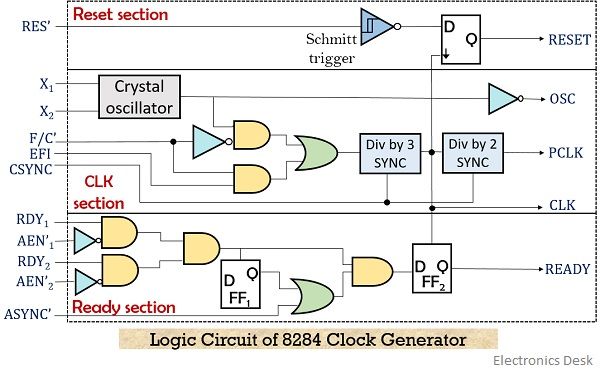
As we can see that the 8284 is composed of 3 sections, reset section, clock section and ready section.
OSC, CLOCK and PCLK are the three outputs generated by the clock section. The crystal oscillator present in this section generates a square wave signal as its output when the crystal is attached between its two inputs X1 and X2.
The frequency of the generated square wave signal is equal to the frequency of the crystal.
Further, the square wave signal is fed to AND gate and NOT gate (inverted buffer) simultaneously. This inverted buffer gives the OSC signal.
- F/C’ is frequency/crystal selection pin used to select the input of the oscillator.
When its input is high then the operating frequency is determined by the external frequency input (EFI), while in the other case it is determined by the crystal oscillator.
Through AND gate, the output of the oscillator is fed to the divided by 3 counter when F/C’ is low. While when F/C’ is high, EFI is fed to the counter. Timing signals for ready and reset pins are produced by the counter.
- For the operation with EFI input, synchronization between multiple processor system is necessary, for which CSYNC is used. Whereas when the crystal oscillator decides the operating frequency then, in that case, this signal is subjected to ground.
CSYNC allows synchronization among multiple 8284s. In the case of single 8284, this pin is grounded.
It is to be noted that the generated output clock frequency in both cases will be one-third of the applied input frequency.
The clock signal for peripheral devices is generated by dividing the clock frequency by 2. Basically, the devices like 8254 timers require PCLK as they need lower operating frequency.
The reset section of 8284 is composed of a Schmitt trigger and a D flip-flop. On each negative edge of the clock signal, the circuit applies a reset signal to the processor.
Initially when the power is first applied then the RC circuit gives logic 0 as input to the RES pin as shown in the figure below. But soon the capacitor gets charged to +5 V through the resistor.
Also, the operator can anytime reset the processor by making use of the push button.
The ready signals for the processor is produced by the ready section. This gives information regarding whether the processor is ready for operation or not. If the ready signal is low, then this shows the wait state of the processor.
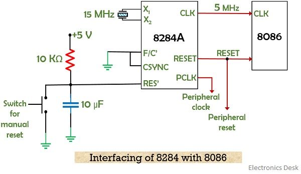
The figure below represents the interfacing of 8284 clock generator with 8086 microprocessor:
Pin Description of 8284
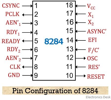
- CSYNC – pin number 1 – Stands for clock synchronization. It is an active high signal that synchronizes the clock signal of various 8284 chips present in a single system. As this pin shows the significance of EFI based operation, thus it is grounded when the crystal is present between the inputs X1 and X2.
- PCLK– pin number 2 – Stands for peripheral clock. An active high signal at this pin provides clock signal of one-sixth frequency of the EFI or crystal frequency to the peripheral devices like 8254.
- AEN1’ and AEN2’ – pin number 3 and 7 – Stands for address enable and are active low pins. It qualifies the bus ready signals i.e., RDY1 and RDY 2.
- RDY1 and RDY 2 – pin number 4 and 6 – These are active high pins and these signals are provided by devices present on the data bus showing the availability or reception of the data.
- READY – pin number 5 – This pin holds the READY signal of 8086 microprocessor.
- CLK – pin number 8 – Stands for clock. The signal frequency at this pin will be one-third to the EFI/crystal frequency having a duty cycle of 33%. It is connected to the clock input of the processor.
- RESET – Pin number 10 – This pin provides the reset signal to the processor and peripheral devices, it is an active-high pin.
- RES’ – Pin number 11 – It is an active low pin that produces a reset signal for 8284. The pin is connected to the RC network for providing power on reset.
- OSC – pin number 12 – It is the output signal of the oscillator with a frequency equal to the applied EFI or crystal frequency.
- F/C’ – pin number 13 – This pin is used to select whether the input used is EFI or crystal for clock generation. For EFI input the pin is connected to VCC i.e., logic high, while for crystal input, the pin is connected to GND.
- EFI – pin number 14 – Stands for external frequency input. This pin provides external input frequency to 8284 when F/C’ is high. The external signal provided at this pin must have frequency thrice that of required clock frequency.
- ASYNC’ – pin number 15 – This pin gives the information regarding the synchronization provided to the inputs. It is an active low pin then two-stage synchronization is provided, otherwise for active high signal, single-stage synchronization is provided.
- X1, X2 – pin number 16 and 17 – These two are the input pins of 8284 and is required while connecting quartz crystal. When EFI is provided then X1 is connected with VCC or GND.
- VCC – pin number 18 – The supply input of +5 V is provided at this pin.
- GND – pin number 9 – This pin is used for the ground connection.
A noteworthy point over here is that, whether the input signal frequency to be given is EFI or crystal, the applied frequency must be three times the required clock frequency at the output.