Definition: A PNP transistor is an acronym used for a positive-negative-positive transistor. It a mainly a classification of bipolar junction transistor and is a three terminal device consisting of the emitter, base and collector.
Here, majority charge carriers are holes and hence they are responsible for the flow of current through the device.
In PNP transistor, an n-type semiconductor is fixed between 2 p-type semiconductor material in order to generate a PNP transistor. It is almost similar to another type of BJT i.e., NPN transistor. However, carriers for current conduction and biasing arrangement generates the difference.
PNP transistor is a current controlled device. As a small amount of base current is responsible for controlling a large emitter-collector voltage. It is to be noted here that like NPN transistor here also the emitter region is highly doped than the base and collector region.
Symbol of PNP Transistor
The figure below shows the symbolic representation of the PNP transistor:
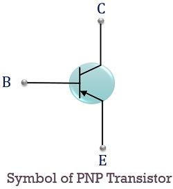
Here, the inward arrow from the emitter to base represents the direction of current conduction.
Construction of PNP Transistor
As we have already discussed that a PNP transistor is formed when 2 p-type semiconductors are connected with an n-type semiconductor material. The semiconductor material can be silicon or germanium.
The figure below shows the structural arrangement of the PNP transistor having 3 regions:
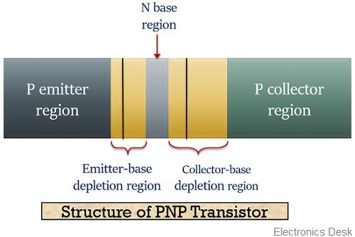
The three regions can be formed by either gaseous diffusion of p-type and n-type impurities on a semiconductor wafer or by an epitaxial method, in which an intrinsic region is grown on the heavily doped substrate of similar material.
Here, the p region is heavily doped than the base and collector region. But the size of the emitter region is greater than the base but comparatively smaller than the collector.
The base region is the thinnest among all and hence least doped. The collector region has the largest area among all but is not doped as high as the emitter.
Like NPN transistor, a PNP transistor is also a back to back connection of two diodes. The figure below shows the connection of two diodes:
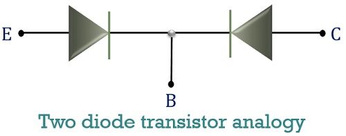
But it is noteworthy here that, we cannot form a transistor by connecting two back to back diodes. Now, the question appears why this is so?
The answer to the above question is that we know that in order to ensure the proper working of the transistor, the doping level of all the 3 regions must be sincerely taken into consideration. But, by connecting two diodes only to have two pn junctions will not give desired transistor operation.
Also, a basic circuit arrangement of the transistor must have a configuration in such a way that emitter-base junction must be forward biased and collector base junction to be reverse biased in order to exhibit diffusion of carriers.
Whereas, in the case of 2 back to back connected diodes, one junction will be forward biased and other will be reverse biased. Hence, diffusion will not take place.
Working of PNP Transistor
As we are already aware of the fact that a PNP transistor comprises 2 p regions and an n region. Therefore, holes are the majority charge carriers and hence responsible for the current conduction.
Now, we will see how the flow of holes generates an electric current through the transistor. The figure below shows the biasing arrangement of the PNP transistor:
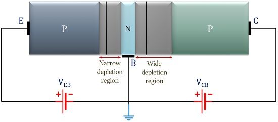
Here, the above figure clearly indicates the emitter-base junction is provided with forward voltage as p region is connected with positive and n region is connected with the negative terminal of the battery.
While the collector-base junction is biased with reverse potential as the p region showing collector is connected with the negative terminal of the battery. This biasing arrangement is necessary so as ensure the operation of the device in the active region.
Let us now see how this biasing arrangement allows current conduction.
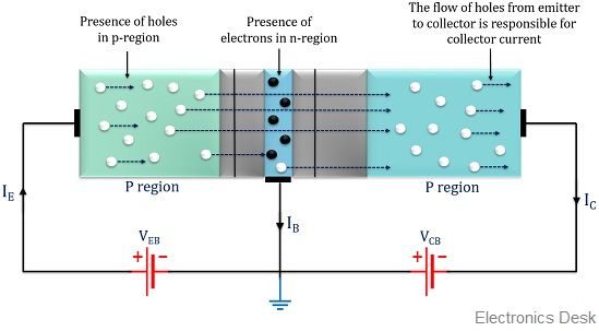
As the emitter region is highly doped so the majority carriers of the p region i.e., holes get repelled by the forward emitter-base voltage. This positive side of the battery applies a repulsive force to the holes and they get sufficient energy and drift across the emitter-base junction and reaches the base region.
As the base region is not highly doped and consists of electrons as the region majority carriers. Thus, only some of the holes reaching the base region combine with the electrons of the base region. Rest, move towards the collector region.
Also, there exists a depletion region due to the base-collector junction of the transistor. The holes moving with high velocity due to the repulsive force of battery VBE drift across the collector region.
At the same time, the negative terminal of the battery VCB also attracts the positively charged holes. The movement of holes in this way generates a large collector current through the device.
It is to be noted here that the emitter current IE is a combination of collector current, IC and base current, IB. This is so because the combination of some of the holes with the electrons of the base region also gives rise to small base current.
Hence, the current equation is written as:
IE = IB + IC
As the base current is very small thus we can say that
IE ≈ IC
In this way, current is generated by the movement of holes in a PNP transistor.
In the operation of the transistor, the efficiency of the emitter and the transport factor plays a vital role.
Uses of PNP Transistor
PNP transistors are widely used in switching and amplifying circuits. These also find applications in Darlington circuits as well as applications related to the field of robotics.
Key terms related to PNP Transistor
- Emitter efficiency: The efficiency of the emitter is defined as the ratio of current at the emitter-base junction due to the majority carriers to the overall emitter current. It is denoted by ϒ.
It is given by: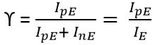
- Transport factor: Transport factor is nothing but the ratio of majority current at the collector junction to the current at the emitter junction. It is given by:

So, from the above discussion, we can conclude that both PNP and NPN are the 2 classifications of BJTs. However, various parameters are present that generates the difference in the operation of the two.