The polarity of the applied external potential (voltage) to any device is characterized as forward and reverse biasing. The crucial difference between forward and reverse biasing is that in forward biasing p region of the device forms a direct connection with the positive side of the battery and n region is connected to the negative side of the battery. As against, in reverse biasing p region of the device forms connection with the negative side of the battery and n region forms a connection with the positive side of the battery.
Any device on the application of external voltage allows it to behave differently. In electronic circuits, mainly the action of electrons and holes is the result of the behaviour of the device.
Let us now see the contents to be discussed under this article and then we will move further to understand other major differences between the two.
Content: Forward Vs Reverse Biasing
Comparison Chart
| Parameter | Forward Biasing | Reverse Biasing |
|---|---|---|
| Current flow | Due to majority charge carriers. | Almost negligible current due to minority charge carriers. |
| Connection Supplied | P region is connected to positive and n region is connected to negative side of the battery. | P region is connected to negative and n region is connected to positive terminal of the battery. |
| Depletion width | Thin | Thick |
| Magnitude of current | High | Low (only leakage current) |
| Operates as | Closed switch | Open switch |
| Barrier potential | Less | More |
| Functioning | Acts as conductor after overcoming potential barrier | Acts as insulator and almost negligible current flows |
| Resistance offered | It offers low resistance. | It offers high resistance. |
| Force experienced by majority carriers | Repulsive | Attractive |
| Diodes that operates on specified biasing | LED, tunnel diode, Shockley diode etc. | Zener diode, varactor diode, photodiode etc. |
Definition of Forward Biasing
A PN junction device is said to be in forward biased condition when the p region forms the connection with positive terminal and n region forms the connection with the negative terminal of the battery.
We already know that in a p-type semiconductor material, holes are present as majority carriers and electrons are present as the minority carriers. While in case of n-type semiconductor material electrons are the majority carriers and holes are the minority carriers.
Let us have a look at the representation of forward biasing applied to a PN junction diode:
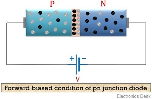
So, when forward biasing is provided to the device as shown above. Then the majority carriers from both sides, i.e., holes from p side and electrons from n side experience a repulsive force from the positive and negative terminal of the battery respectively.
As we already know the Coulomb’s law of physics that like charges repel each other and unlike charges attract each other. So, due to the repulsion from the externally provided supply, the majority carriers gain sufficient energy and overcome the barrier potential. The barrier potential is nothing but a region of neutral atoms that get generated due to temperature difference when no external voltage is provided to it.
With the increase in the applied forward voltage, the width of the depletion region decreases. After completely overcoming the barrier potential, the depletion region diminishes and a sharp flow of current is noticed because a large number of majority carriers now cross the junction region.
Definition of Reverse Biasing
A PN junction device is in reverse biased condition when the p region is connected to the negative potential and n region is connected to the positive potential of the battery.
Let us have a look at the reverse biased arrangement of a PN junction diode:
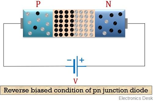
It is clear from the above figure that, the majority carriers present in p region i.e., holes attract towards the negative terminal of the battery. Similarly, electrons in the n region attract towards the positive side of the battery. So, due to this, the majority carriers start moving away from the junction. Resultantly, this increases the depletion width. Due to the increase in the width of the depletion region, the flow of current due to majority carriers somewhat gets restricted.
However, the minority carriers in both the regions i.e., electrons in p side and holes in the n side experience repulsion from the battery terminals and move across the junction. Due to this movement, a very small reverse leakage current flows through the device. This current is known as reverse saturation current. As in reverse biased condition, no any current flows due to the majority carriers through the device. Thus, it is said that it behaves like an insulator.
Key Differences between Forward Biasing and Reverse Biasing
- The factor that generates a key difference between forward biasing and reverse biasing is that when a forward voltage is applied to a device then mainly the current flow due to the movement of majority charge carriers. On the contrary, when a reverse voltage is applied to a device then the movement of only minority carriers generates small current, known as leakage current.
- On applying a forward voltage to a PN junction device the depletion width decreases with the increase in supplied voltage. While, when reverse biasing is provided to a PN junction device then the width of the depletion region increases with supplied voltage.
- Due to forward applied voltage pn junction device acts as a good conductor after overcoming the barrier potential. Whereas, due to reverse supplied voltage pn junction devices start behaving as an insulator thus, allowing almost negligible current flow through it.
- In case of forward applied potential, the PN junction device offers very low resistance. On the other side, in case of reverse applied voltage, pn junction device offers very high resistance.
- It is basically understood that a forward biased voltage permits a large flow of current thus operates as a closed switch. While a reverse biased voltage does not allow sufficient current flow hence fundamentally termed as an open switched condition.
- Due to the thin depletion region at the time of forward biasing, the barrier potential is low. However, due to the thick depletion width in case of reverse biasing, the barrier potential is high.
- In case of forward biasing, majority carriers experience repulsion from the battery terminal. As against, in the case of reverse biasing, majority carriers experience attraction from the terminals of the battery.
Conclusion
So, from the above discussion, we can conclude that the flow of current through a PN junction device depends on the biasing arrangement provided to it. As various factors show dependency on the arrangement of the external voltage provided to it.