IMPATT is an abbreviation used for IMPact ionization Avalanche Transit-Time. IMPATT diode is a very high power semiconductor device that is utilized for microwave applications.
It is basically used as oscillator and amplifier at microwave frequencies. The operating range of the IMPATT diode lies in the range of 3 to 100 GHz.
Basically it possesses negative resistance characteristic thus acts as an oscillator to generate signals at microwave frequencies. It is a reverse-biased diode and Avalanche condition is the basis of its operation.
Content: IMPATT Diode
Construction
The figure here represents the structure of the IMPATT diode:
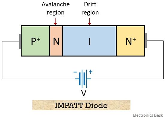
As we can see that it consists of 4 regions namely P+-N-I-N+
The structure of the IMPATT diode is somewhat similar to the PIN diode. However, it operates on a very high voltage gradient of around 400KV/cm, so as to produce avalanche current.
Generally, materials like GaAs, Si, Ge or InP are used for its construction. However, GaAs is preferred because of its low noise behaviour.
Basically, it uses a slightly different structure from a normal diode. Because we know that a normal PN junction diode breaks down under avalanche condition. As the generation of a large amount of current causes the generation of heat inside it.
So variation in construction is adopted to produce RF signals at microwave frequencies.
Working of IMPATT Diode
As we have already discussed that these diodes operate on the principle of avalanche breakdown and transit time delay.
So let’s first understand what is Avalanche Condition(breakdown).
An action that causes an abrupt increase in the junction current in reverse biased condition of pn junction diode leading to junction breakdown is known as avalanche breakdown.
We know that in reverse biased condition the width of the depletion region becomes extremely thick. Due to which only minority carriers drift across the junction. In the presence of a high electric field, the mobile charge carriers move with greater velocity.
During their movement, the high-velocity carriers collide with other atoms in the crystal and generates electron-hole pairs. This causes multiplication of charge carriers inside the crystal structure.
Thus the moving charges generate high current inside the device. This is known as avalanche condition or impact ionization and is utilized in IMPATT diodes.
It is to be noted here that the overall external field provided to the diode is the summation of RF ac signal and dc voltage.
- Initially when ac voltage is 0 then due to applied low dc voltage, a very small amount of current flows through the diode. This current is generally known as pre-breakdown current.
- But as the applied potential increases then the electric field inside the diode increases. And as we have already discussed that with an increase in the electric field there will be an increase in the number of generated electron-hole pairs due to impact ionization.
The above figure clearly shows the avalanche region and drift space in the structure of the diode.
The increase in superimposed ac field and dc potential causes the electrons in the p+ region to get injected into the I region in order to drift towards n+ region. This is so because with the increase in the applied field the electrons will move towards the anode and holes towards the cathode.
The moving electrons cause charge multiplication in the presence of a high electric field.
By this time the ac field now starts approaching 0 but due to secondary charge generation, the concentration of electrons in the avalanche region will be extremely high.
This shows a phase shift of 90⁰ now gets generated between the ac input signal and concentration of charge carriers in the avalanche region.
Thus while drifting from avalanche region to anode, the electrons generate high current with a phase opposite to that of the applied ac signal.
During the negative half of the ac signal, even the dc potential is high, still, the reduction in the overall electric field will cause decay in the concentration of carriers present in the avalanche region. Thus the current flowing through it also gets reduced.
- In order to have the desired phase shift between the ac signal and diode current, the thickness of the drift region must be properly selected.
The thickness of the drift region must be such that the electron bunch must be collected at the anode till the time ac voltage is approaching 0. Thereby providing a phase shift of 90⁰. This is so because the thickness of the drift region decides the time taken by the carriers to reach the respective electrode.
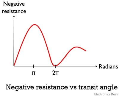
Though all the carriers travel unequal distance while approaching the electrode. But the introduced phase-shift due to drifting generates negative resistance.
The figure below represents the negative resistance characteristic of IMPATT diode with respect to transit angle:
Hence in this way current through an IMPATT diode is generated.
Advantages
- It provides high operating range.
- It shows compactness in size.
- IMPATT diodes are economical.
- It provides reliable operation at high temperature.
Disadvantages
- The rate of generation of electron-hole pair in the avalanche region causes the generation of high noise. Thus makes the system noisy.
- It offers a low tuning range.
- It offers high sensitivity to different operating conditions.
Applications
IMPATT diodes find applications in microwave oscillators, parametric amplifiers and microwave generators. Along with these, other uses involve presence in intruder alarm systems, telecommunication transmitters and receivers etc.