Definition: 8051 is an 8-bit microcontroller that contains 40 pins of dual-in-line packaging. Out of the 40 pins, 32 pins are allotted to I/O ports. However, in 8051 there exist multiple pins which are assigned more than one signal.
We have already discussed the architecture and working of 8051 microcontrollers. In the working, we have already mentioned that it has 4 parallel ports of 8 bits each. Thereby forming a configuration of 32 pins in the pin description.
Now the question arises, how the same pin can be configured differently?
So, the logic state of the pin decides whether the pin is operating in input or output mode. Thus, we can say logic 1 at the I/O port configures the pin as an input. While logic 0 at the I/O port shows the enabling of output.
Let us now move further to understand the pin configuration of 8051 microcontrollers.
Pin Diagram of 8051 Microcontroller
The figure below shows the pin diagram of 8051 microcontroller:
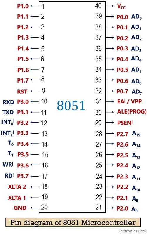 As we can see in the figure shown above that the pin diagram consists of 40 pins in its configuration. Out of the 40 pins, 32 pins are assigned to I/O ports. But only a single bank of 8 pins are not used in conjunction with other pins. While the rest 24 ports are used with pins of different functionality.
Let us now discuss the functioning of each pin in detail.
Pin Description of 8051 Microcontroller
VCC – Pin number 40 – 8051 operates on +5 V of the supply voltage. Thus this pin is solely assigned to VCC at which the supply voltage is provided.
GND – Pin number 20 – This pin is allotted to ground, that passes the excess current of the microcontroller to the ground.
Port 0 – Pin number 32 to 39 – These eight pins acts as bidirectional I/O ports as well as multiplexed data and address bus. These input and output lines are used for the accessing of external memory.
Here lower order address and data bus (i.e., AD0 to AD7) are multiplexed together with the I/O ports. Port 0 do not hold any internal pull-ups, so in order to use it as I/O port, external pull-ups are required.
The pin when gets enabled shows the accessing of data from the desired address of external memory. Hence port 0 is utilized as a multiplexed address/data bus.
Port 1 – Pin number 1 to 8 – These pins are assigned specifically to bidirectional I/O ports including the internal pull-ups and are used for any other functioning in 8051 IC.
Port 2 – Pin number 21 to 28 – These pins are assigned bidirectional I/O port 2. Also when external memory is needed to be accessed then these pins act as higher order address bus (i.e., A8 to A15).
Port 3 – Pin number 10 to 17 – These pins are bidirectional I/O ports. Along with this, all the pins in port 3 acts as multipurpose pins.
This means despite serving as I/O port, these pins also hold some special function, which is stated below:
P3.0 (RXD) – Pin number 10 – This pin is used for serial port to receive the data in UART mode. While in shift register mode it acts as data I/O pin.
P3.1 (TXD) – Pin number 11 – This is another pin for serial port that is used to transmit data in UART mode. However, in shift register mode, it acts as clock output.
P3.2 (INT0‘) – Pin number 12 – It is the interrupt 0 input pin which shows the presence of an interrupt when an active low signal is generated at this pin.
P3.3 (INT1‘) – Pin number 13 – It is an interrupt 1 input pin, which when goes active low shows the existence of interrupt in the system.
P3.4 (T0) – Pin number 14 – This pin is assigned to timer 0 of the microcontroller. An active high signal at this pin indicates that the system is producing a time delay.
P3.5 (T1) – Pin number 15 – As we have already discussed in the architecture of 8051 microcontrollers, that it has 2 timers. So, this pin is allotted to timer 1.
P3.6 (WR’) – Pin number 16 – This pin gets active whenever a write operation is performed. More specifically we can say, an active low signal at this pin indicates that write operation is being executed at the external memory.
P3.7 (RD’)– Pin number 17 – This pin is used to show the read operation. Basically, the hardware generates an active low signal at the pin for the case of read operation from the external memory.
XTAL 2 and XTAL 1 – Pin number 18 and 19 respectively – These two pins are allotted for internal clock signalling. The external oscillator forms a connection to these two pins so as to have an internal clock signal to the system.
RST – Pin number 9 – This pin gets active high whenever; the microcontroller is required to be set to its initial state. Basically, in order to have proper reset operation of the microcontroller, at the time of running oscillator, this pin signal must be kept high for two consecutive machine cycle.
PSEN| – Pin number 29 – PSEN is an abbreviation for program store enable. An active low signal at this pin shows that read operation is being executed from external program memory i.e., ROM/EPROM.
ALE – Pin number 30 – It is an address latch enable pin. An active high signal at this pin represents the presence of address in the multiplexed address and data bus. The enabling of this pin provides information to memory and peripheral devices about the fetching of the data from the desired address.
EA|/ VPP – Pin number 31 – Here EA is used for External Access. Whenever there is a need to access the program from external memory, then signal at this pin must be active low. While in case the code is not accessed by the external memory then it has an active high signal.
Sometimes when flash programming is executed in the microcontroller, then programming enable voltage of 12 V is applied at this pin.
This is all about the pin diagram and pin description of 8051 microcontrollers.