Pentium Microprocessor is one of the powerful family members of Intel’s Χ86 microprocessor. It is an advanced superscalar 32-bit microprocessor, introduced in the year 1993 that contains around 3.1 million transistors.
It has a 64-bit data bus and a 32-bit address bus that offers 4 Gb of physical memory space. While the maximum clock rating offered is around 60 to 233 MHz.
Content: Pentium Microprocessor
Introduction
The architectural representation of the Pentium processor is considered to be an advancement of 80386 and 80486 microprocessors. Basically, Pentium has included modifications related to cache structure, the width of the data bus, numeric coprocessor with faster speed along with providing dual integer processor.
In the case of a Pentium processor, there are two caches, one for caching data while another for caching information and each one is of 8K size. By using a dual integer processor, two instructions can be executed in each clock cycle. The data bus width in Pentium is 64-bit which was 32-bit in 80386 and the numeric coprocessor exhibits quite a faster speed than that of 80486.
However, an advancement to Pentium was Pentium pro that is comparatively faster than the former. The reason behind this is that its architecture allows scheduling 5 simultaneous instructions in order to get executed. Along with level-1 cache i.e., 16K-byte like Pentium, it has a level-2 cache that offers 256K-byte size. Not only this, Pentium pro has an error correction unit that offers correction of single-bit error and detection of two-bit error. With the use of additional four address lines, the Pentium pro offers 64 Gb of accessible physical memory.
Features of Pentium Processor
Following are the features that Pentium processor offers:
- Superscalar architecture
- Separate data and instruction caches
- Bus cycle pipelining
- Execution tracing
- 64-bit data bus
- Internal parity checking
- Dynamic branch prediction
- Dual processing support
- Performance monitoring
We have already mentioned in the beginning that Pentium is a superscalar processor. So, let us first understand
What are Superscalar Processors?
A special category of microprocessors that involves a parallel approach for instruction execution called instruction-level parallelism through which more than one instruction gets executed in one clock cycle is called superscalar processors. It is famous as a second-generation RISC processor because RISC is the ones that operate in a faster manner with reduced instruction sets.
Unlike scalar processors that have the ability to execute maximal one instruction per clock cycle, the superscalar processor uses the approach of simultaneously executing two instructions in one clock cycle. The superscalar processors perform this task by sending multiple instructions to various execution units at the same time. Hence this provides high throughput.
It is to be noted here that superscalar processors are generally pipelined. However, pipelining is different from super scaling in a way that superscalars allow execution of multiple instructions parallelly using multiple execution units while pipelining uses a single execution unit which is divided into multiple phases in order to execute multiple instructions.
Architecture of Pentium Microprocessor
The figure given here is the architectural representation of Pentium Processor:
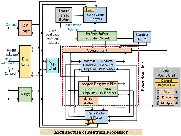
The various functional units are as follows:
- Bus unit
- Paging unit
- Control ROM
- Prefetch buffer
- Execution unit with two integer pipeline (U-pipe and V-pipe)
- Code cache
- Data cache
- Instruction decode
- Branch target buffer
- Dual processing logic
- Advanced programmable interrupt controller
Let us now understand, how the architectural operation takes place.
The bus unit of the architecture sends the control signal and fetches cade and data from external memory and IO devices. The size of the external data bus is 64-bit through which burst read and burst write-back cycles can be achieved. The paging unit in the architecture provides optional extensions of around 2 to 4 Mb page sizes.
In order to load the instructions into the execution unit, code cache, branch target buffer and prefetch buffers operate together. The code cache or the external memory holds the instructions from where these are fetched. While the branch target buffer holds the address of the respective branch and the TLB (translational lookaside buffer) within the code cache converts the linear address into the physical address that is used by the code cache.
This processor contains pairs of prefetch buffers having a size of 32-byte that combinedly operate with branch target buffer. Both the buffers operate independently but not at the same time. One of the prefetch buffers starts fetching the instructions in a sequential manner till the time branch instruction has not occurred. However, as soon as the branch instruction is fetched by the prefetch buffer then BTB will check for the branch but once it is checked by BTB that branch has not occurred then linear fetching of instruction will continue.
On the contrary, while checking if BTB gets to know about the occurrence of the branch then the other prefetch buffer in pair gets enabled and starts fetching the instructions from the branch target address. By doing so, the branching instructions get simultaneously fetched and are ready for decoding and execution.
The execution unit within the Pentium microprocessor contains two integer pipelines namely U-pipe and V-pipe and each one has its separate ALU. There are five stages in which these pipelines operate, namely, prefetch, decode-1, decode-2, execute, writeback. The U-pipe is responsible for executing all integer as well as floating-point instructions while V-pipe executes simple integer and some floating-point instructions.
Here, the instruction fetch reads the instruction one at a time and stores them in the instruction queue. During the execution of an instruction, the processor does not sit idle and checks for the next two instructions in the queue. If the two instructions are independent of each other then U-pipe and V-pipe are assigned instructions individually so that execution can occur simultaneously. However, in the case, the queued instructions are dependent on each other then both the instructions are assigned to U-pipe for execution one after the other and V-pipe remains idle.
The controlling of the operations of the Pentium processor is provided by the control ROM that has a microcode within it. The control ROM directly controls U-pipe and V-pipe.
Both data and code cache within the processor is organized in the 2-way associated set cache. Each cache has 128 sets and each set has 2 lines which are 32 bytes wide. The LRU (Least Recently Used) mechanism handles the cache replacement.
As we can see clearly in the above figure that the code cache forms a connection with the prefetch buffer by a bus of size 256 bit, thus 256/8 i.e., 32 bytes of opcode can be buffered in one clock cycle. The data cache has two ports that are used to simultaneously deal with two data references.
There is an on-chip Advanced Programmable Interrupt Controller that manages interrupt and offers 8259A compatibility.
Here we have discussed the basic Pentium processor model, however, Intel also released multiple advanced processors that include advanced features after Pentium. The various Pentium series are Pentium Pro, Pentium II, Pentium III, and Pentium 4 processors.